• Menu
  • Product
  • Email
  • PDF
  • Order now
  • TPS6109x Synchronous Boost Converter With 2-A Switch

    • SLVS484C June   2003  – December 2014 TPS61090 , TPS61091 , TPS61092

      PRODUCTION DATA.  

  • CONTENTS
  • SEARCH
  • TPS6109x Synchronous Boost Converter With 2-A Switch
  1. 1 Features
  2. 2 Applications
  3. 3 Description
  4. 4 Revision History
  5. 5 Device Comparison Table
  6. 6 Pin Configuration and Functions
  7. 7 Specifications
    1. 7.1 Absolute Maximum Ratings
    2. 7.2 ESD Ratings
    3. 7.3 Recommended Operating Conditions
    4. 7.4 Electrical Characteristics
    5. 7.5 Typical Characteristics
  8. 8 Parameter Measurement Information
  9. 9 Detailed Description
    1. 9.1 Overview
    2. 9.2 Functional Block Diagram
    3. 9.3 Feature Description
      1. 9.3.1 Synchronous Rectifier
      2. 9.3.2 Controller Circuit
      3. 9.3.3 Device Enable
      4. 9.3.4 Undervoltage Lockout
      5. 9.3.5 Softstart
      6. 9.3.6 Power Save Mode and Synchronization
      7. 9.3.7 Low Battery Detector Circuit—LBI/LBO
      8. 9.3.8 Low-EMI Switch
    4. 9.4 Device Functional Modes
  10. 10Application and Implementation
    1. 10.1 Application Information
    2. 10.2 Typical Applications
      1. 10.2.1 Typical Application Circuit for Adjustable Output Voltage Option
        1. 10.2.1.1 Design Requirements
        2. 10.2.1.2 Detailed Design Procedure
          1. 10.2.1.2.1 Programming the Output Voltage
          2. 10.2.1.2.2 Programming the LBI/LBO Threshold Voltage
          3. 10.2.1.2.3 Inductor Selection
          4. 10.2.1.2.4 Capacitor Selection
            1. 10.2.1.2.4.1 Input Capacitor
            2. 10.2.1.2.4.2 Output Capacitor DC-DC Converter
            3. 10.2.1.2.4.3 Small Signal Stability
        3. 10.2.1.3 Application Curves
      2. 10.2.2 TPS6109x Application Schematic of 5 Vout With Maximum Output Power
      3. 10.2.3 TPS6109x Application Schematic of 5 Vout and Auxiliary 10 Vout With Charge Pump
      4. 10.2.4 TPS6109x Application Schematic of 5 Vout and Auxiliary -5 Vout With Charge Pump
  11. 11Power Supply Recommendations
  12. 12Layout
    1. 12.1 Layout Guidelines
    2. 12.2 Layout Example
    3. 12.3 Thermal Considerations
  13. 13Device and Documentation Support
    1. 13.1 Device Support
      1. 13.1.1 Third-Party Products Disclaimer
    2. 13.2 Related Links
    3. 13.3 Trademarks
    4. 13.4 Electrostatic Discharge Caution
    5. 13.5 Glossary
  14. 14Mechanical, Packaging, and Orderable Information
  15. IMPORTANT NOTICE
search No matches found.
  • Full reading width
    • Full reading width
    • Comfortable reading width
    • Expanded reading width
  • Card for each section
  • Card with all content


DATA SHEET

TPS6109x Synchronous Boost Converter With 2-A Switch

1 Features

  • Synchronous (96% Efficient) Boost Converter With 500-mA Output Current From 1.8-V Input
  • Available in a 16-Pin VQFN 4 x 4 Package
  • Device Quiescent Current: 20 µA (Typ)
  • Input Voltage Range: 1.8 V to 5.5 V
  • Adjustable Output Voltage Up to 5.5 V Fixed Output Voltage Options
  • Power Save Mode for Improved Efficiency at Low Output Power
  • Low Battery Comparator
  • Low EMI-Converter (Integrated Antiringing Switch)
  • Load Disconnect During Shutdown
  • Over-Temperature Protection

2 Applications

  • All Single Cell Li or Dual Cell Battery or USB Powered Operated Products
    • MP3 Player
    • PDAs
    • Other Portable Equipment

3 Description

The TPS6109x devices provide a power supply solution for products powered by either a one-cell Li-Ion or Li-Polymer, or a two-cell alkaline, NiCd or NiMH battery and required supply currents up to or higher than 1 A. The converter generates a stable output voltage that is either adjusted by an external resistor divider or fixed internally on the chip. It provides high efficient power conversion and is capable of delivering output currents up to 0.5 A at 5 V at a supply voltage down to 1.8 V. The implemented boost converter is based on a fixed frequency, pulse-width- modulation (PWM) controller using a synchronous rectifier to obtain maximum efficiency. Boost switch and rectifier switch are connected internally to provide the lowest leakage inductance and best EMI behavior possible. The maximum peak current in the boost switch is limited to a value of 2500 mA.

The converter can be disabled to minimize battery drain. During shutdown, the load is completely disconnected from the battery. A low-EMI mode is implemented to reduce ringing and, in effect, lower radiated electromagnetic energy when the converter enters the discontinuous conduction mode.

The output voltage can be programmed by an external resistor divider or is fixed internally on the chip.

The device is packaged in a 16-pin VQFN 4-mm x 4-mm (16 RSA) package.

Device Information(1)

PART NUMBER PACKAGE BODY SIZE (NOM)
TPS61090 VQFN (10) 4.00 mm × 4.00 mm
TPS61091
TPS61092
  1. For all available packages, see the orderable addendum at the end of the datasheet.

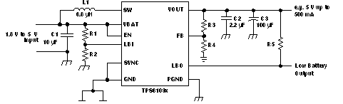
Simplified Application Schematic

typ_app_fp_LVS484.gif

4 Revision History

Changes from B Revision (April 2005) to C Revision

  • Added Pin Configuration and Functions section, ESD Ratings table, Feature Description section, Device Functional Modes, Application and Implementation section, Power Supply Recommendations section, Layout section, Device and Documentation Support section, and Mechanical, Packaging, and Orderable Information section Go

5 Device Comparison Table

TA OUTPUT VOLTAGE DC-DC(1) PACKAGE PART NUMBER(2)
40°C to 85°C Adjustable 16-pin VQFN 4 mm × 4 mm TPS61090RSA
3.3 V 16-pin VQFN 4 mm × 4 mm TPS61091RSA
5 V 16-pin VQFN 4 mm × 4 mm TPS61092RSA
(1) Contact the factory to check availability of other fixed output voltage versions.
(2) See Mechanical, Packaging, and Orderable Information for ordering information and tape and reel options.


Texas Instruments

© Copyright 1995-2025 Texas Instruments Incorporated. All rights reserved.
Submit documentation feedback | IMPORTANT NOTICE | Trademarks | Privacy policy | Cookie policy | Terms of use | Terms of sale