-
UCC2897A Advanced Current-Mode Active-Clamp PWM Controller
- 1 Features
- 2 Applications
- 3 Description
- 4 Revision History
- 5 Device Options
- 6 Pin Configuration and Functions
- 7 Specifications
-
8 Detailed Description
- 8.1 Overview
- 8.2 Functional Block Diagram
- 8.3 Feature Description
- 8.4 Device Functional Modes
- 9 Application and Implementation
- 10Power Supply Recommendations
- 11Layout
- 12Device and Documentation Support
- 13Mechanical, Packaging, and Orderable Information
- IMPORTANT NOTICE
UCC2897A Advanced Current-Mode Active-Clamp PWM Controller
1 Features
- Low-output jitter
- Soft-stop shutdown of MAIN and AUX
- 110-V input startup function
- Ideal for active-clamp, reset-forward, flyback and synchronous rectifier uses
- Provides complementary auxiliary driver with programmable dead time (Turn-On Delay) between AUX and MAIN switches
- Peak current-mode control with 0.5-V cycle-by-cycle current limiting
- TrueDrive™ 2-A Sink, 2-A source outputs
- Trimmed internal-bandgap reference for accurate line UV and line OV threshold
- Programmable slope compensation
- High-performance 1-MHz synchronizable oscillator with internal timing capacitor
- Precise programmable maximum duty cycle
- PB-free lead finish package
2 Applications
- High-efficiency DC-to-DC power supplies
- Server power, 48-V telecom, datacom, and 42-V automotive applications
3 Description
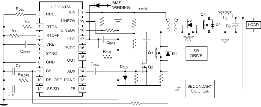
The UCC2897A PWM controller simplifies implementation of the various active clamp or reset and synchronous rectifier switching power topologies.
The UCC2897A is a peak current-mode fixed-frequency high-performance pulse-width modulator. The controller includes the logic and the drive capability for the P-channel auxiliary switch along with a simple method of programming the critical delays for proper active-clamp operation.
Features include an internal programmable slope compensation circuit, precise DMAX limit, and a synchronizable oscillator with an internal-timing capacitor. An accurate line-monitoring function also programs the ON and OFF transitions of the converter with regard to the bulk input voltage, VIN.
The UCC2897A adds a second-level hiccup-mode current-sense threshold, bi-directional synchronization and input-overvoltage protection functionalities. The UCC2897A is offered in 20-pin TSSOP (PW) and 20-pin QFN (RGP) packages.
Device Information(1)
| PART NUMBER | PACKAGE | BODY SIZE (NOM) |
|---|---|---|
| UCC2897A | TSSOP (20) | 6.60 mm x 6.60 mm |
| VQFN (20) | 4.15 mm x 4.15 mm |
- For all available packages, see the orderable addendum at the end of the datasheet.
