-
UCC28019A 8-Pin Continuous Conduction Mode (CCM) PFC Controller
- 1 Features
- 2 Applications
- 3 Description
- 4 Revision History
- 5 Pin Configuration and Functions
- 6 Specifications
-
7 Detailed Description
- 7.1 Overview
- 7.2 Functional Block Diagram
- 7.3
Feature Description
- 7.3.1 Soft-Start
- 7.3.2
System Protection
- 7.3.2.1 VCC Undervoltage Lockout (UVLO)
- 7.3.2.2 Input Brown-Out Protection (IBOP)
- 7.3.2.3 Output Overvoltage Protection (OVP)
- 7.3.2.4 Open Loop Protection/Standby (OLP/Standby)
- 7.3.2.5 ISENSE Open-Pin Protection (ISOP)
- 7.3.2.6 Output Undervoltage Detection (UVD) and Enhanced Dynamic Response (EDR)
- 7.3.2.7 Over-Current Protection
- 7.3.2.8 Soft Over Current (SOC)
- 7.3.2.9 Peak Current Limit (PCL)
- 7.3.2.10 Current Sense Resistor, RISENSE
- 7.3.3 Gate Driver
- 7.3.4 Current Loop
- 7.3.5 ISENSE and ICOMP Functions
- 7.3.6 Pulse Width Modulator
- 7.3.7 Control Logic
- 7.3.8 Voltage Loop
- 7.3.9 Output Sensing
- 7.3.10 Voltage Error Amplifier
- 7.3.11 Non-Linear Gain Generation
- 7.4 Device Functional Modes
- 8 Application and Implementation
- 9 Power Supply Recommendations
- 10Layout
- 11Device and Documentation Support
- 12Mechanical, Packaging, and Orderable Information
- IMPORTANT NOTICE
UCC28019A 8-Pin Continuous Conduction Mode (CCM) PFC Controller
1 Features
- 8-Pin Solution Reduces External Components
- Wide-Range Universal AC Input Voltage
- Fixed 65-kHz Operating Frequency
- Maximum Duty Cycle of 98% (typ.)
- Output Over/Undervoltage Protection
- Input Brown-Out Protection
- Cycle-by-Cycle Peak Current Limiting
- Open Loop Detection
- Low-Power User-Controlled Standby Mode
2 Applications
- CCM Boost Power Factor Correction Power Converters in the 100 W to >2 kW Range
- Digital TV
- Home Electronics
- White Goods and Industrial Electronics
- Server and Desktop Power Supplies
3 Description
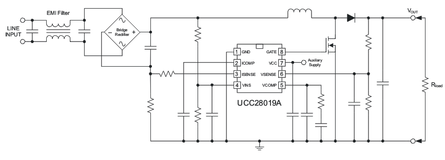
The UCC28019A 8-pin active Power Factor Correction (PFC) controller uses the boost topology operating in Continuous Conduction Mode (CCM). The controller is suitable for systems in the 100 W to >2 kW range over a wide-range universal ac line input. Start-up current during undervoltage lockout is less than 200 μA. The user can control low power standby mode by pulling the VSENSE pin below 0.77 V.
Low-distortion wave shaping of the input current using average current mode control is achieved without input line sensing, reducing the external component count. Simple external networks allow for flexible compensation of the current and voltage control loops. The switching frequency is internally fixed and trimmed to better than ±5% accuracy at 25°C. Fast 1.5-A peak gate current drives the external switch.
Numerous system-level protection features include peak current limit, soft over-current, open-loop detection, input brown-out, and output over/undervoltage. Soft-start limits boost current during start-up. A trimmed internal reference provides accurate protection thresholds and a regulation set-point. An internal clamp limits the gate drive voltage to 12.5 V.
Device Information(1)
| PART NUMBER | PACKAGE | BODY SIZE (NOM) |
|---|---|---|
| UCC28019A | SOIC (8) | 3.91 mm × 4.9 mm |
| PDIP (8) | 6.35 mm × 9.81 mm |
- For all available packages, see the orderable addendum at the end of the data sheet.
Simplified Schematic
4 Revision History
Changes from C Revision (August 2015) to D Revision
Changes from B Revision (April 2009) to C Revision
- Added ESD Ratings table, Feature Description section, Device Functional Modes, Application and Implementation section, Power Supply Recommendations section, Layout section, Device and Documentation Support section, and Mechanical, Packaging, and Orderable Information section. Go
5 Pin Configuration and Functions
Pin Functions
| PIN | I/O | DESCRIPTION | |
|---|---|---|---|
| NAME | NO. | ||
| SOIC, PDIP | |||
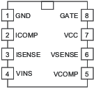
| GND | 1 | — | Ground: device ground reference. |
| ICOMP | 2 | O | Current loop compensation: Transconductance current amplifier output. A capacitor connected to GND provides compensation and averaging of the current sense signal in the current control loop. The controller is disabled if the voltage on ICOMP is less than 0.6 V. |
| ISENSE | 3 | I | Inductor current sense: Input for the voltage across the external current sense resistor, which represents the instantaneous current through the PFC boost inductor. This voltage is averaged by the current amplifier to eliminate the effects of ripple and noise. Soft Over Current (SOC) limits the average inductor current. Cycle-by-cycle Peak Current Limit (PCL) immediately shuts off the GATE drive if the peak-limit voltage is exceeded. An internal 1.5-μA current source pulls ISENSE above 0.1 V to shut down PFC operation if this pin becomes open-circuited. Use a 220-Ω resistor between this pin and the current sense resistor to limit inrush-surge currents into this pin. |
| VINS | 4 | I | Input ac voltage sense: A filtered resistor-divider network connects from this pin to the rectified-mains node. Input Brown-Out Protection (IBOP) detects when the system ac-input voltage is above a user-defined normal operating level, or below a user-defined “brown-out” level. At startup the controller is disabled until the VINS voltage exceeds a threshold of 1.5 V, initiating a soft start. The controller is also disabled if VINS drops below the brown-out threshold of 0.8 V. Operation will not resume until both VINS and VSENSE voltages exceed their enable thresholds, initiating another soft start. |
| VCOMP | 5 | O | Voltage loop compensation: Transconductance voltage error amplifier output. A resistor-capacitor network connected from this pin to GND provides compensation. VCOMP is held at GND until VCC, VINS, and VSENSE all exceed their threshold voltages. Once these conditions are satisfied, VCOMP is charged until the VSENSE voltage reaches 99% of its nominal regulation level. When Enhanced Dynamic Response (EDR) is engaged, a higher transconductance is applied to VCOMP to reduce the charge time for faster transient response. Soft Start is programmed by the capacitance on this pin. The EDR higher transconductance is inhibited during Soft Start. |
| VSENSE | 6 | I | Output voltage sense: An external resistor-divider network connected from this pin to the PFC output voltage provides feedback sensing for regulation to the internal 5-V reference voltage. A small capacitor from this pin to GND filters high-frequency noise. Standby mode disables the controller and discharges VCOMP when the voltage at VSENSE drops below the enable threshold of 0.8 V. An internal 100-nA current source pulls VSENSE to GND for Open-Loop Protection (OLP), including pin disconnection. Output Over-Voltage Protection (OVP) disables the GATE output when VSENSE exceeds 105% of the reference voltage. Enhanced Dynamic Response (EDR) rapidly returns the output voltage to its normal regulation level when a system line or load step causes VSENSE to fall below 95% of the reference voltage. |
| VCC | 7 | Device supply: External bias supply input. Under-Voltage Lockout (UVLO) disables the controller until VCC exceeds a turn-on threshold of 10.5 V. Operation continues until VCC falls below the turn-off (UVLO) threshold of 9.5 V. A ceramic by-pass capacitor of 0.1 μF minimum value should be connected from VCC to GND as close to the device as possible for high frequency filtering of the VCC voltage. | |
| GATE | 8 | O | Gate drive: Integrated push-pull gate driver for one or more external power MOSFETs. Typical 2.0-A sink and 1.5-A source capability. Output voltage is typically clamped at 12.5 V. |
6 Specifications
6.1 Absolute Maximum Ratings(1)
Over operating free-air temperature range unless otherwise noted. Unless noted, all voltages are with respect to GND. Currents are positive into and negative out of the specified terminal.| MIN | MAX | UNIT | ||
|---|---|---|---|---|
| Input voltage range | VCC, GATE | –0.3 | 22 | V |
| VINS, VSENSE, | –0.3 | 7 | V | |
| VCOMP, ICOMP(2) | –0.3 | 7.5 | V | |
| ISENSE | –24 | 7 | V | |
| Input current range | VSENSE, ISENSE | –1 | 1 | mA |
| Lead temperature, TSOL | Soldering, 10s | 300 | °C | |
| Junction temperature, TJ | Operating | –55 | 150 | °C |
| Storage | –65 | 150 | °C | |
6.2 ESD Ratings
| VALUE | UNIT | |||
|---|---|---|---|---|
| V(ESD) | Electrostatic discharge | Human-body model (HBM), per ANSI/ESDA/JEDEC JS-001(1) | ±2000 | V |
| Charged-device model (CDM), per JEDEC specification JESD22-C101(2) | ±500 | V | ||
6.3 Recommended Operating Conditions
over operating free-air temperature range (unless otherwise noted)| MIN | MAX | UNIT | |
|---|---|---|---|
| VCC input voltage from a low-impedance source | VCCOFF + 1 V | 21 | V |
| Operating junction temperature, TJ | -40 | 125 | °C |
6.4 Thermal Information
| THERMAL METRIC(1) | UCC28019A | UNIT | ||
|---|---|---|---|---|
| P (PDIP) | D (SOIC) | |||
| 8 PINS | 8 PINS | |||
| RθJA | Junction-to-ambient thermal resistance | 52.8 | 113.0 | °C/W |
| RθJC(top) | Junction-to-case (top) thermal resistance | 42.3 | 61.5 | °C/W |
| RθJB | Junction-to-board thermal resistance | 30.0 | 53.2 | °C/W |
| ψJT | Junction-to-top characterization parameter | 19.5 | 15.9 | °C/W |
| ψJB | Junction-to-board characterization parameter | 29.9 | 52.7 | °C/W |
6.5 Electrical Characteristics
Unless otherwise noted, VCC=15 VDC, 0.1 μF from VCC to GND, -40°C ≤ TJ = TA ≤ 125°C. All voltages are with respect to GND. Currents are positive into and negative out of the specified terminal.| PARAMETER | TEST CONDITION | MIN | TYP | MAX | UNIT | |
|---|---|---|---|---|---|---|
| VCC Bias Supply | ||||||
| ICCPRESTART | ICC pre-start current | VCC = VCCON – 0.1 V | 25 | 100 | 200 | μA |
| ICCSTBY | ICC standby current | VSENSE = 0.5 V | 1 | 2.2 | 2.9 | mA |
| ICCON_load | ICC operating current | VSENSE = 4.5 V, CGATE = 4.7 nF | 4 | 7.5 | 10 | mA |
| Under Voltage Lockout (UVLO) | ||||||
| VCCON | VCC turn on threshold | 10 | 10.5 | 11 | V | |
| VCCOFF | VCC turn off threshold | 9 | 9.5 | 10 | V | |
| UVLO hysteresis | 0.8 | 1 | 1.2 | V | ||
| Oscillator | ||||||
| fSW | Switching frequency | TA = 25°C | 61.7 | 65 | 68.3 | kHz |
| -25°C ≤ TA ≤ 125°C | 59 | 65 | 71 | kHz | ||
| -40°C ≤ TA ≤ 125°C | 57 | 71 | kHz | |||
| PWM | ||||||
| DMIN | Minimum duty cycle | VCOMP = 0 V, VSENSE = 5 V, ICOMP = 6.4 V |
0% | |||
| DMAX | Maximum duty cycle | VSENSE = 4.95 V | 94% | 98% | 99.3% | |
| tOFF(min) | Minimum off time | VSENSE = 3 V, ICOMP = 1 V | 100 | 250 | 600 | ns |
| System Protection | ||||||
| VSOC | ISENSE threshold, Soft Over Current (SOC) | -0.66 | -0.73 | -0.79 | V | |
| VPCL | ISENSE threshold, Peak Current Limit (PCL) | -1 | -1.08 | -1.15 | V | |
| IISOP | ISENSE bias current, ISENSE Open-Pin Protection (ISOP) | ISENSE = 0 V | -2.1 | -4.0 | μA | |
| VISOP | ISENSE threshold, ISENSE Open-Pin Protection (ISOP) | ISENSE = open pin | 0.082 | V | ||
| VOLP | VSENSE threshold, Open Loop Protection (OLP) | ICOMP = 1 V, ISENSE = -0.1 V, VCOMP = 1 V |
0.77 | 0.82 | 0.86 | V |
| Open Loop Protection (OLP) Internal pull-down current | VSENSE = 0.5 V | 100 | 250 | nA | ||
| VUVD | VSENSE threshold, output Under-Voltage Detection (UVD)(1) | 4.63 | 4.75 | 4.87 | V | |
| VOVP | VSENSE threshold, output Over-Voltage Protection (OVP) | ISENSE = -0.1 V | 5.12 | 5.25 | 5.38 | V |
| VINSBROWNOUT_th | Input Brown-Out Detection (IBOP) high-to-low threshold |
0.76 | 0.82 | 0.88 | V | |
| VINSENABLE_th | Input Brown-Out Detection (IBOP) low-to-high threshold |
1.4 | 1.5 | 1.6 | V | |
| IVINS_0V | VINS bias current | VINS = 0 V | 0 | ±0.1 | μA | |
| ICOMP threshold, external overload protection | 0.6 | V | ||||
| Current Loop | ||||||
| gmi | Transconductance gain | TA = 25°C | 0.75 | 0.95 | 1.15 | mS |
| Output linear range(1) | ±50 | μA | ||||
| ICOMP voltage during OLP | VSENSE = 0.5 V | 3.7 | 4 | 4.3 | V | |
| Voltage Loop | ||||||
| VREF | Reference voltage | -40°C ≤ TA ≤ 125°C | 4.9 | 5 | 5.1 | V |
| gmv | Transconductance gain without EDR | -31.5 | -42 | -52.5 | μS | |
| gmv-EDR | Transconductance gain under EDR | VSENSE = 4.65 V | -440 | μS | ||
| Maximum sink current under normal operation | VSENSE = 6 V, VCOMP = 4 V | 21 | 30 | 38 | μA | |
| Source current under soft start | VSENSE = 4 V, VCOMP = 2.5 V | -21 | -30 | -38 | μA | |
| Maximum source current under EDR operation | VSENSE = 4 V, VCOMP = 2.5 V | -300 | μA | |||
| VSENSE = 4 V, VCOMP = 4 V | -170 | μA | ||||
| Enhanced dynamic response VSENSE low threshold, falling(1) | 4.63 | 4.75 | 4.87 | V | ||
| VSENSE input bias current | VSENSE = 5 V | 20 | 100 | 250 | nA | |
| VCOMP voltage during OLP | VSENSE = 0.5 V, IVCOMP = 0.5 mA | 0 | 0.2 | 0.4 | V | |
| VCOMP rapid discharge current | VCOMP = 3 V, VCC = 0 V | 0.77 | mA | |||
| VPRECHARGE | VCOMP precharge voltage | IVCOMP = -100 μA, VSENSE = 5 V | 1.76 | V | ||
| IPRECHARGE | VCOMP precharge current | VCOMP = 1.0 V | -1 | mA | ||
| VSENSE threshold, end of soft start | Initial start up | 4.95 | V | |||
| GATE Driver | ||||||
| GATE current, peak, sinking(1) | CGATE = 4.7 nF | 2 | A | |||
| GATE current, peak, sourcing(1) | CGATE = 4.7 nF | -1.5 | A | |||
| GATE rise time | CGATE = 4.7 nF, GATE = 2 V to 8 V | 8 | 40 | 60 | ns | |
| GATE fall time | CGATE = 4.7 nF, GATE = 8 V to 2 V | 8 | 25 | 40 | ns | |
| GATE low voltage, no load | I GATE = 0 A | 0 | 0.05 | V | ||
| GATE low voltage, sinking | I GATE = 20 mA | 0.3 | 0.8 | V | ||
| GATE low voltage, sourcing | I GATE = -20 mA | -0.3 | -0.8 | V | ||
| GATE low voltage, sinking, device OFF | VCC = 5 V, IGATE = 5 mA | 0.2 | 0.75 | 1.2 | V | |
| VCC = 5 V, IGATE = 20 mA | 0.2 | 0.9 | 1.5 | V | ||
| GATE high voltage | VCC = 20 V, CGATE = 4.7 nF | 11.0 | 12.5 | 14.0 | V | |
| VCC = 11 V, CGATE = 4.7 nF | 9.5 | 10.5 | 11.0 | V | ||
| VCC = VCCOFF + 0.2 V, CGATE = 4.7 nF | 8.0 | 9.4 | 10.2 | V | ||
6.6 Typical Characteristics
Unless otherwise noted, VCC = 15 VDC, 0.1 μF from VCC to GND, -40°C ≤ TJ = TA ≤ 125°C. All voltages are with respect to GND. Currents are positive into and negative out of the specified terminal.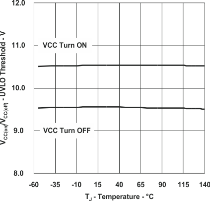 Figure 1. UVLO Thrasholds vs Temperature
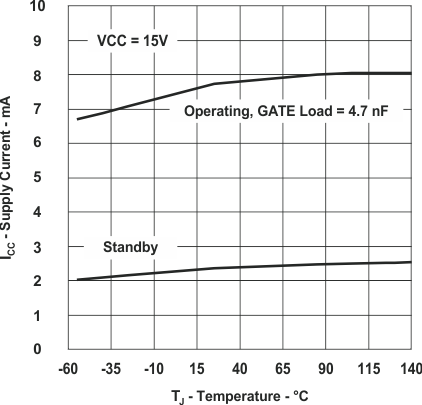 Figure 3. Supply Current vs Temperature
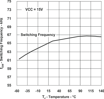 Figure 5. Oscillator Frequency vs Temperature
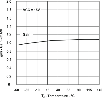 Figure 7. Current Averaging Amplifier Transconductance vs Temperature
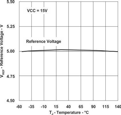 Figure 9. Reference Voltage vs Temperature
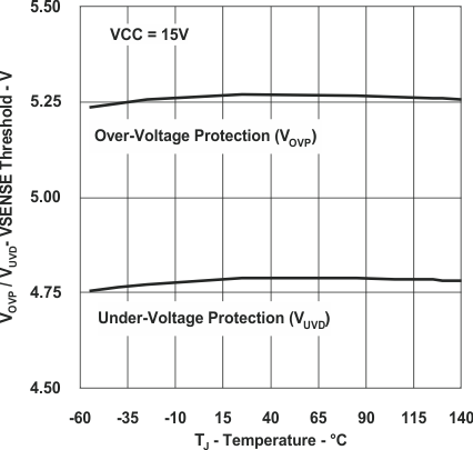 Figure 11. VSENSE Threshold vs Temperature
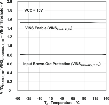 Figure 13. VINS Threshold vs Temperature
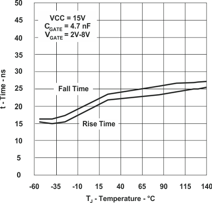 Figure 15. Gate Drive Switching vs Temperature
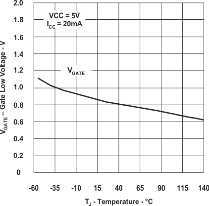 Figure 17. Gate Low Voltage With Device Off vs Temperature
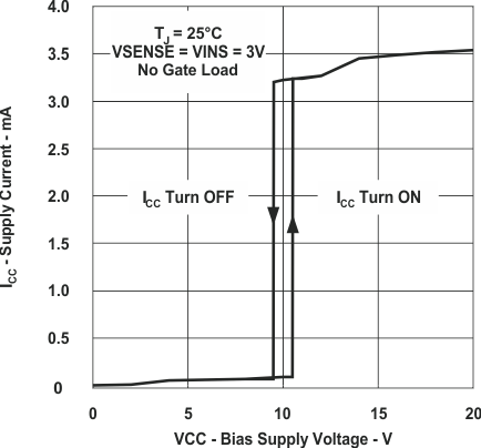 Figure 2. Supply Current vs Bias Supply Voltage
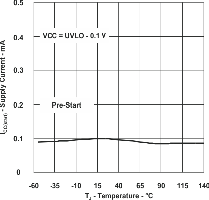 Figure 4. Supply Current vs Temperature
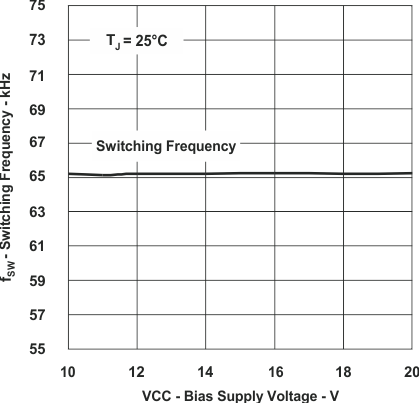 Figure 6. Oscillator Frequency vs Bias Supply Voltage
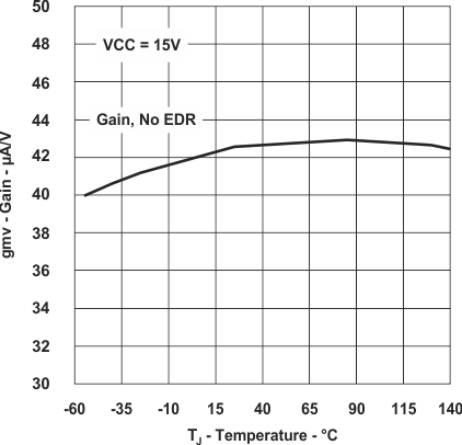 Figure 8. Voltage Error Amplifier Transconductance vs Temperature
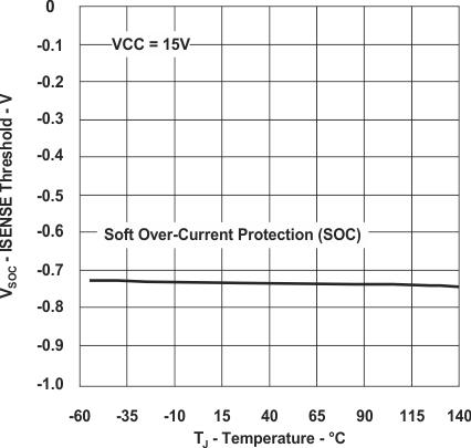 Figure 10. ISENSE Threshold vs Temperature
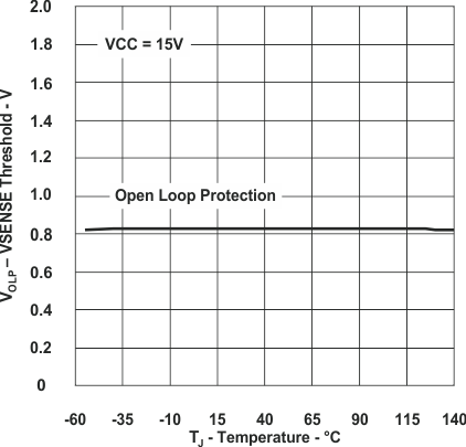 Figure 12. VSENSE Threshold vs Temperature
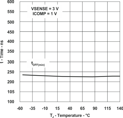 Figure 14. Minimum Off Time vs Temperature
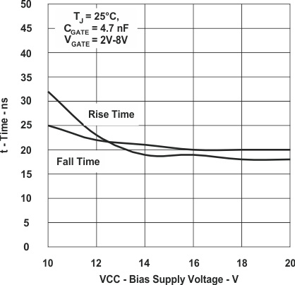 Figure 16. Gate Drive Switching vs Bias Supply Voltage