TPS51120 Dual, Synchronous Step-Down Controller With 100-mA Standby Regulators for Notebook System Power
1 Features
- 3.3-V and 5-V 100-mA Bootstrapped Standby Regulators with Independent Enables
- Selectable D-CAP™ Mode Enables Fast Transient Response Less than 100 ns
- Selectable Low Ripple Current Mode
- Less than 1% Internal Reference Accuracy
- Selectable PWM-only/Auto-skip Modes
- Low-side RDS(on) Loss-less Current Sensing
- RSENSE Accurate Current Sense Option
- Internal Soft-Start and Integrated VOUT Discharge Transistors
- Integrated 2-V Reference
- Adaptive Gate Drivers with Integrated Boost Diode
- Powergood for Each Channel with Delay Timer
- Fault Disable Mode
- Supply Input Voltage Range: 4.5 V to 28 V
2 Applications
Notebook Computers System Bus and I/O
3 Description
The TPS51120 is a highly sophisticated dual, synchronous step-down controller. It is a full featured controller designed to run directly off a three- or four-cell Li-ion battery and provide high-power and 5-V and/or 3.3-V standby regulation for all the downstream circuitry in a notebook computer system. High-current, 100-mA, 5-V or 3.3-V on-board linear regulators have glitch-free switch over function to SMPS and can be kept alive independently during standby state. The pseudo-constant frequency adaptive on-time control scheme supports full range of current mode operation including simplified loop compensation, ceramic output capacitors as well as seamless transition to reduced frequency operation at light-load condition. Optional D-CAP mode operation optimized for SP-CAP or POSCAP output capacitors allows further reduction of external compensation parts. Dynamic UVP supports VIN line sag without latch off by hitting 5-V UVP. No negative voltage appears at output voltage node during UVLO, UVP, and OCP, OTP or loss of VIN.
The TPS51120 32-pin QFN package is specified from –40°C to 85°C ambient temperature.
Device Information(1)
| PART NUMBER | PACKAGE | BODY SIZE (NOM) |
|---|---|---|
| TPS51120 | VQFN (32) | 5.00 mm × 5.00 mm |
- For all available packages, see the orderable addendum at the end of the datasheet.
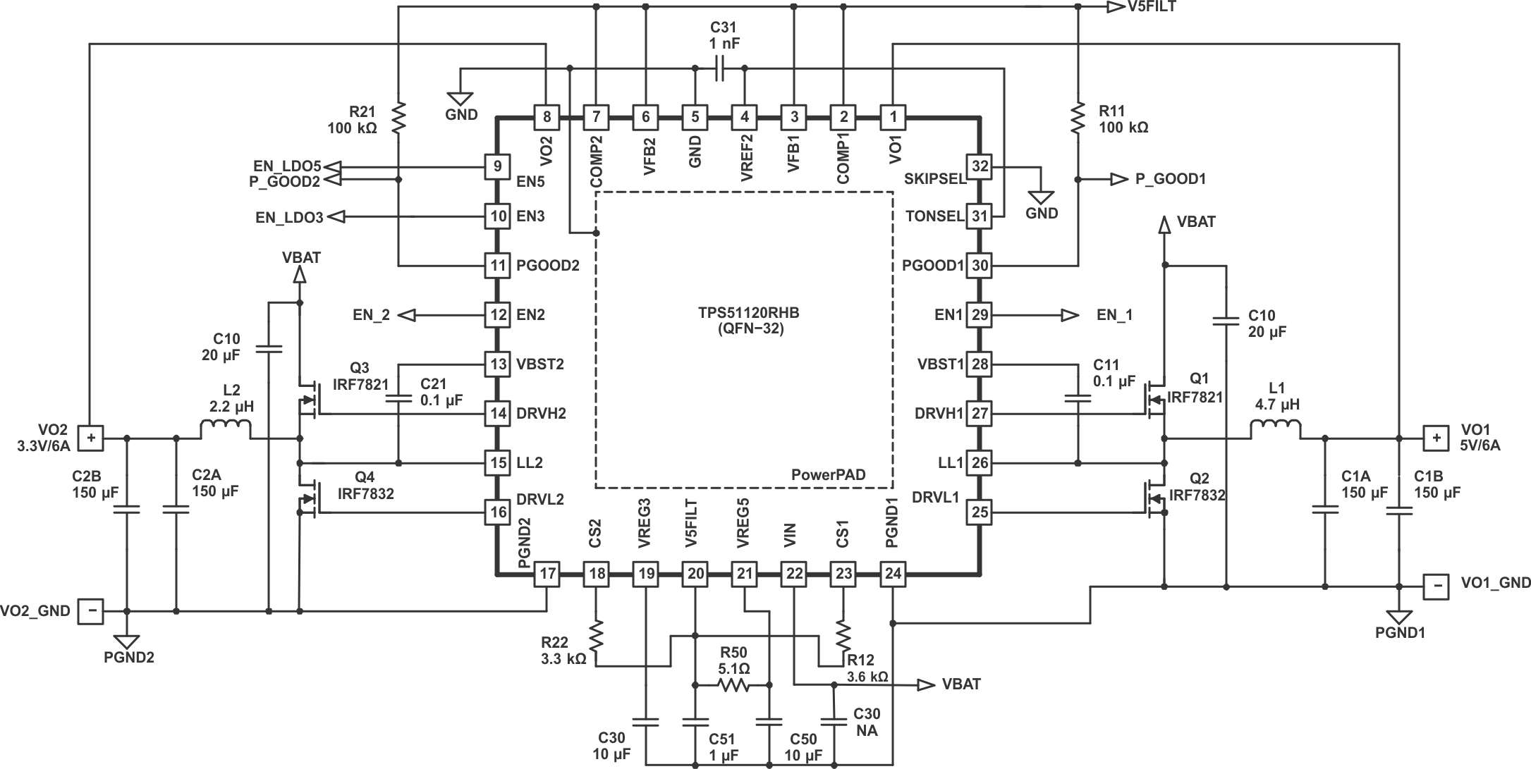
Reference Design for D-CAP Mode Converter
4 Revision History
Changes from B Revision (Feburary 2007) to C Revision
- Added Pin Configuration and Functions section, Feature Description section, Device Functional Modes, Application and Implementation section, Power Supply Recommendations section, Layout section, Device and Documentation Support section, and Mechanical, Packaging, and Orderable Information section Go
5 Pin Configuration and Functions
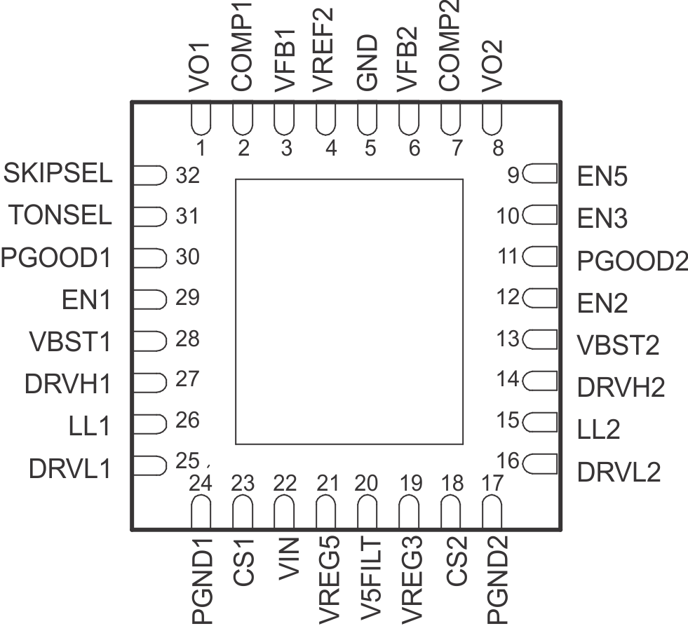
Pin Functions
| PIN | I/O | DESCRIPTION | |
|---|---|---|---|
| NAME | NO. | ||
| COMP1 | 2 | O | Loop compensation pin (error amplifier output). Connect RC from this pin to GND for proper loop compensation with current mode operation. Tie this pin to V5FILT for D-CAP mode operation. |
| COMP2 | 7 | O | |
| CS1 | 23 | I | Current sense comparator input (-) for resistor sensing scheme. Or, overcurrent trip setting input for RDS(on) current sense scheme if connected to V5FILT through the threshold setting resistor. |
| CS2 | 18 | I | |
| DRVH1 | 27 | O | High-side MOSFET gate drive output. Source 3.5 Ω, sink 1.5 Ω, LL-node referenced floating driver. Drive voltage corresponds to VBST to LL voltage. |
| DRVH2 | 14 | O | |
| DRVL1 | 25 | O | Rectifying (low-side) MOSFET gate drive output. Source 3.5 Ω, sink 1.5 Ω, PGND referenced driver. Drive voltage is VREG5 voltage. |
| DRVL2 | 16 | O | |
| EN1 | 29 | I | Channel 1 and Channel 2 SMPS enable pins. Connect to 5 V to turn on with internal 3-ms soft-start. Slower soft-start is possible by applying an external capacitor from each of these pins to ground to program ramp rate. |
| EN2 | 12 | I | |
| EN3 | 10 | I | VREG3, 3.3-V low dropout linear regulator enable pin. Connect to GND to disable. Float or tie to enabled VREG5 to turn on the regulator. |
| EN5 | 9 | I | VREG5, 5-V low dropout linear regulator enable pin. Connect to GND to disable. Float or tie to VBAT to turn on the regulator. |
| GND | 5 | I | Signal ground pin. |
| LL1 | 26 | I/O | High-side MOSFET gate driver return. Also serve as current sense comparator input (-) for RDS(on) sensing, and input voltage monitor for on-time control circuitry |
| LL2 | 15 | I/O | |
| PGND1 | 24 | I/O | Ground return for rectifying MOSFET gate driver. Connect PGND2, PGND1 and GND strongly together near the source of the rectifying FET or the GND connection of the current sense resistor. Also serve as current sense comparator input (+). |
| PGND2 | 17 | I/O | |
| PGOOD1 | 30 | O | Power-good window comparator open drain output. Pull up with resistor to V5FILT or appropriate signal voltage. Current capability is 5-mA. PGOOD goes high 1-ms after VFB is within specified limits. Power bad (terminal goes low) is within 10 μs. |
| PGOOD2 | 11 | O | |
| SKIPSEL | 32 | I | Skip and fault mode selection pin. Refer to Table 5 |
| TONSEL | 31 | I | On-time selection pin. Refer to Table 1 and Table 5. |
| V5FILT | 20 | I | 5-V supply input for the entire control circuit. Should be provided from VREG5 via RC filter. |
| VBST1 | 28 | I | Supply Input for High-side MOSFET Driver. Connect capacitor from this pin to respective LL terminal. An internal PN diode is connected between VREG5 to each of these pins. User can add external schottky diode if forward drop is critical to drive the power MOSFET. |
| VBST2 | 13 | I | |
| VFB1 | 3 | I | SMPS feedback input. Connect the feedback resistor divider here for adjustable outputs. Tie these pins to V5FILT or for fixed output option. Refer to Table 5 |
| VFB2 | 6 | I | |
| VIN | 22 | I | Supply Input for 5-V and 3.3-V linear regulator. Typically connected to VBAT. |
| VO1 | 1 | I | These terminals serve four functions: on-time adjustment, output discharge, VREG5, VREG3 switchover input and feedback inputs for 5-V, 3.3-V fixed-output option. Connect to positive terminal of respective switch mode power supply’s output capacitor. |
| VO2 | 8 | I | |
| VREF2 | 4 | O | 2-V reference output. Capable of ±50-μA, ±2% over 0 - 85°C temperature range. Bypass to GND by 1-nF ceramic capacitor. Tie this pin to GND disables both SMPS. |
| VREG3 | 19 | O | 3.3-V, 100-mA low dropout linear regulator output. Bypass to PGND by 10-μF ceramic capacitor. Runs from VIN supply. Shuts off with EN3. Switches over to VO2 when 3.1 V or above is provided. |
| VREG5 | 21 | O | 5-V, 100-mA low dropout linear regulator output. Bypass to PGND by 10-μF ceramic capacitor. Runs from VIN supply. Internally connected to VBST and DRVL. Shuts off with EN5. Switches over to VO1 when 4.8 V or above is provided. |