-
THS4509 Wideband, Low-Noise, Low-Distortion, Fully-Differential Amplifier
- 1 Features
- 2 Applications
- 3 Description
- 4 Revision History
- 5 Device Comparison Table
- 6 Pin Configuration and Functions
- 7 Specifications
- 8 Detailed Description
- 9 Application and Implementation
- 10Power Supply Recommendations
- 11Layout
- 12Device and Documentation Support
- 13Mechanical, Packaging, and Orderable Information
- IMPORTANT NOTICE
THS4509 Wideband, Low-Noise, Low-Distortion, Fully-Differential Amplifier
1 Features
- Fully-Differential Architecture
- Centered Input Common-Mode Range
- Output Common-Mode Control
- Minimum Gain of 2 V/V (6 dB)
- Bandwidth: 1900 MHz
- Slew Rate: 6600 V/μs
- 1% Settling Time: 2 ns
- HD2: –75 dBc at 100 MHz
- HD3: –80 dBc at 100 MHz
- OIP3: 37 dBm at 70 MHz
- Input Voltage Noise: 1.9 nV/√Hz (f > 10 MHz)
- Power-Supply Voltage: 3 V to 5 V
- Power-Supply Current: 37.7 mA
- Power-Down Current: 0.65 mA
2 Applications
- 5-V Data Acquisition Systems High
Linearity ADC Amplifiers - Wireless Communication
- Medical Imaging
- Test and Measurement
3 Description
The THS4509 device is a wideband, fully-differential op amp designed for 5-V data acquisition systems. It has a low noise at 1.9 nV/√Hz, and low harmonic distortion of –75 dBc HD2 and –80 dBc HD3 at 100 MHz with 2 VPP, G = 10 dB, and 1-kΩ load. Slew rate is high at 6600 V/μs, and with settling time of 2 ns to 1% (2-V step), it is ideal for pulsed applications. It is designed for a minimum gain of 6 dB, but is optimized for gains of 10 dB.
To allow for DC coupling to analog-to-digital converters (ADCs), its unique output common-mode control circuit maintains the output common-mode voltage within 3-mV offset (typical) from the set voltage, when set within 0.5-V of midsupply, with less than 4-mV differential offset voltage. The common-mode set point is set to midsupply by internal circuitry, which may be overdriven from an external source.
The input and output are optimized for best performance with the common-mode voltages set to midsupply. Along with high performance at low power-supply voltage, this design makes it ideal for high-performance, single-supply 5-V data acquisition systems. The combined performance of the THS4509 in a gain of 10 dB driving the ADS5500 ADC, sampling at 125 MSPS, is 81-dBc SFDR and
69.1-dBc SNR with a –1 dBFS signal at 70 MHz.
The THS4509 is offered in a quad, leadless VQFN-16 package (RGT), and is characterized for operation over the full industrial temperature range from –40°C to +85°C.
Device Information(1)
| PART NUMBER | PACKAGE | BODY SIZE (NOM) |
|---|---|---|
| THS4509 | VQFN (16) | 3.00 mm × 3.00 mm |
- For all available packages, see the orderable addendum at the end of the data sheet.
4 Revision History
Changes from H Revision (November 2009) to I Revision
- Added ESD Ratings table, Thermal Information table, Feature Description section, Device Functional Modes, Application and Implementation section, Power Supply Recommendations section, Layout section, Device and Documentation Support section, and Mechanical, Packaging, and Orderable Information section.Go
- Deleted the Packaging/Ordering Information table, see POA at the end of the data sheet Go
- Deleted the THS4509 EVM section to the Layout Example section Go
Changes from G Revision (May 2008) to H Revision
- Changed title of Typical Characteristics: VS+ – VS– = 5 VGo
- Deleted conditions from Typical Characteristics: VS+ – VS– = 5 V table of graphsGo
- Changed title of Typical Characteristics: VS+ – VS– = 3 VGo
- Deleted conditions from Typical Characteristics: VS+ – VS– = 3 V table of graphsGo
- Added y-axis to Figure 87Go
- Added y-axis to Figure 90Go
- Changed item 10 in Layout Recommendations sectionGo
- Added the PowerPAD PCB Layout Considerations sectionGo
- Moved Figure 92 and associated paragraph to PowerPAD PCB Layout Considerations sectionGo
- Added the PowerPAD Design Considerations sectionGo
Changes from F Revision (October 2007) to G Revision
- Updated document formatGo
- Changed common-mode range column for THS4509 and THS4513 rows in the Related Products tableGo
- Added footnote 1 to Absolute Maximum Ratings tableGo
- Added V (volts) to unit column of ESD ratings rows in Absolute Maximum Ratings tableGo
- Changed VS+ – VS– = 5 V Input specifications from 1.75 V typ (common-mode input range high) to 1.4 V typ; –1.75 V (common-mode input range low) to –1.4 V; 1.35 MΩ || 1.77 pF (differential input impedance) to 1.3 MΩ || 1.8 pF; 1.02 MΩ || 2.26 pF (common-mode input impedance) to 1.0 MΩ || 2.3 pFGo
- Changed VS+ – VS– = 3 V Input specifications from 0.75 V typ (common-mode input range high) to 0.4 V typ; –0.75 V (common-mode input range low) to –0.4 V; 1.35 MΩ || 1.77 pF (differential input impedance) to 1.3 MΩ || 1.8 pF; 1.02 MΩ || 2.26 pF (common-mode input impedance) to 1.0 MΩ || 2.3 pFGo
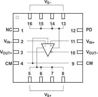
6 Pin Configuration and Functions

Pin Functions
| PIN | TYPE | DESCRIPTION | |
|---|---|---|---|
| NAME | NO. | ||
| NC | 1 | N/A | No internal connection |
| VIN– | 2 | I | Inverting amplifier input |
| VOUT+ | 3 | O | Noninverting amplifier output |
| CM | 4, 9 | I | Common-mode voltage input |
| VS+ | 5-8 | P | Positive amplifier power-supply input |
| VOUT– | 10 | O | Inverted amplifier output |
| VIN+ | 11 | I | Noninverting amplifier input |
| PD | 12 | I | Power-down; PD = logic low puts part into low power mode, PD = logic high or open for normal operation |
| VS– | 13, 14, 15, 16 | P | Negative amplifier power-supply input |

