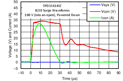
-
TPD1S414 USB Charger Overvoltage, Surge, and ESD Protection for VBUS Pin
- 1 Features
- 2 Applications
- 3 Description
- 4 Revision History
- 5 Pin Configuration and Functions
-
6 Specifications
- 6.1 Absolute Maximum Ratings
- 6.2 ESD Ratings
- 6.3 Recommended Operating Conditions
- 6.4 Thermal Information
- 6.5 Electrical Characteristics (EN, ACK Pins)
- 6.6 Electrical Characteristics (OVP Circuit)
- 6.7 Timing Requirements
- 6.8 Switching Characteristics (nFET)
- 6.9 Supply Current Consumption
- 6.10 Thermal Shutdown Feature
- 6.11 Typical Characteristics
-
7 Detailed Description
- 7.1 Overview
- 7.2 Functional Block Diagram
- 7.3
Feature Description
- 7.3.1 Overvoltage Protection on VBUS_CON up to 30-V DC
- 7.3.2 Low RON nFET Switch Supports Host and Charging Mode
- 7.3.3 ±15-kV IEC 61000-4-2 Level 4 ESD Protection
- 7.3.4 100-V IEC 61000-4-5 µs Surge Protection
- 7.3.5 Start-Up and OVP Recovery Delay
- 7.3.6 Integrated Input Enable and Status Output Signal
- 7.3.7 Thermal Shutdown
- 7.4 Device Functional Modes
- 8 Application and Implementation
- 9 Power Supply Recommendations
- 10Layout
- 11Device and Documentation Support
- 12Mechanical, Packaging, and Orderable Information
- IMPORTANT NOTICE
TPD1S414 USB Charger Overvoltage, Surge, and ESD Protection for VBUS Pin
1 Features
- Overvoltage Protection at VBUS_CON Up to 30-V DC
- Low RON nFET Switch Supports Host and Charging Mode
- Internal 15-ms Start-Up Delay
- Internal 30-ms Soft-Start Delay to Minimize the USB Inrush Current
- Transient Protection for VBUS Line:
- IEC 61000-4-2 Contact Discharge ±15 kV
- IEC 61000-4-2 Air Gap Discharge ±15 kV
- IEC 61000-4-5 Open-Circuit Voltage 100 V
- Integrated Input Enable and Status Output Signal
- Thermal Shutdown (TSD) Feature
- Space-Saving DSBGA Package: (1.4 mm × 1.89 mm)
2 Applications
- End Equipment
- Mobile Phones
- Tablets
- Wearables
- Electronic-Point-of-Sale (EPOS)
- Interfaces
- USB 2.0
- USB 3.0
- USB Type C
3 Description
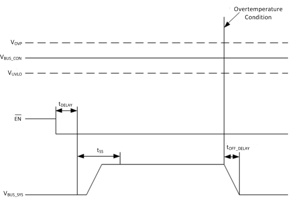
The TPD1S414 device is a single-chip solution for a USB connector’s VBUS line protection. The bidirectional nFET switch ensures safe current flow in both charging and host mode while protecting the internal system circuits from any overvoltage conditions at the VBUS_CON pin. On the VBUS_CON pin, this device can handle overvoltage protection up to 30 V. After the EN pin toggles low, the TPD1S414 waits 20 ms before turning ON the nFET through a soft-start delay. ACK pin indicates the FET is completely turned ON.
The typical application interface for the TPD1S414 is the VBUS line in USB connectors. Typical end equipment for TPD1S414 are mobiles phones, tablets, wearables, and electronic-point-of-sale (EPOS). The TPD1S414 can also be applied to any system using an interface with a 5-V power rail.
Device Information(1)
| PART NUMBER | PACKAGE | BODY SIZE (NOM) |
|---|---|---|
| TPD1S414 | DSBGA (12) | 1.40 mm × 1.89 mm |
- For all available packages, see the orderable addendum at the end of the data sheet.
Typical Application Schematic
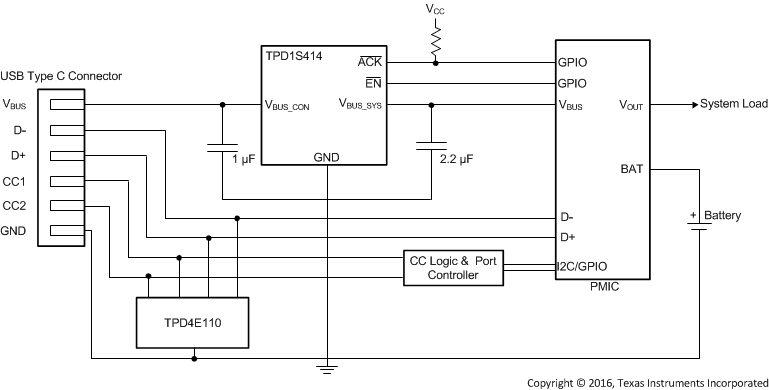
4 Revision History
Changes from A Revision (October 2013) to B Revision
- Added ESD Ratings table, Detailed Description section, Application and Implementation section, Power Supply Recommendations section, Device and Documentation Support section, and Mechanical, Packaging, and Orderable Information sectionGo
Changes from * Revision (October 2013) to A Revision
- Changed text in the DESCRIPTION From: TPD1S414 waits 15 ms before turning ON the nFET To: TPD1S414 waits 20 ms before turning ON the nFETGo
- Deleted Continuous forward current through the FET body diode, IDIODE from the ABSOLUTE MAXIMUM RATINGS tableGo
- Deleted Peak input current on VBUS_CON pin, IBUS from the ABSOLUTE MAXIMUM RATINGS tableGo
- Added Voltage on ACK pin to the ABSOLUTE MAXIMUM RATINGS tableGo
- Added Continuous current on VBUS_CON and VBUS_SYS pins to the RECOMMENDED OPERATING CONDITIONS tableGo
- Added Continuous forward current through the FET body diode, IDIODE to the RECOMMENDED OPERATING CONDITIONS tableGo
- Added values to the THERMAL INFORMATION tableGo
- Changed the IHOST_LEAK MAX value From: 160 To: 200 µA in the SUPPLY CURRENT CONSUMPTION tableGo
- Deleted graphs: Enabling the Load Switch, Connecting VBUS_CON, and OVP Operation from the TIMING DIAGRAMS sectionGo
- Changed horizontal axis labeling on Figure 7Go
- Changed Figure 10Go
- Added text to the APPLICATION INFORMATION sectionGo
5 Pin Configuration and Functions
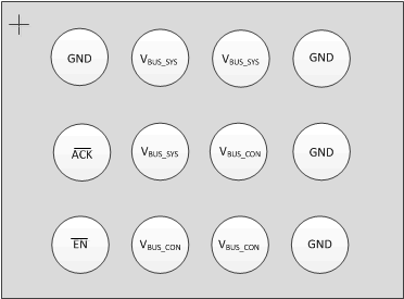
Pin Functions
| PIN | TYPE | DESCRIPTION | |
|---|---|---|---|
| NAME | NO. | ||
| ACK | B1 | O | Open-Drain Acknowledge pin. See Table 2. |
| EN | C1 | I | Enable Active-Low Input. Drive EN low to enable the switch. Drive EN high to disable the switch. |
| VBUS_CON | B3, C2, C3 | I/O | Connect to USB connector VBUS pin; IEC61000-4-2 ESD protection IEC61000-4-5 Surge protection |
| VBUS_SYS | A2, A3, B2 | I/O | Connect to internal VBUS plane |
| GND | A1, A4, B4, C4 | Ground | Connect to PCB ground plane |
Table 1. 12-YZ Pin Mapping
| 1 | 2 | 3 | 4 | |
|---|---|---|---|---|
| A | GND | VBUS_SYS | VBUS_SYS | GND |
| B | ACK | VBUS_SYS | VBUS_CON | GND |
| C | EN | VBUS_CON | VBUS_CON | GND |
6 Specifications
6.1 Absolute Maximum Ratings
over operating free-air temperature range (unless otherwise noted)(1)(2)6.2 ESD Ratings
| VALUE | UNIT | ||||
|---|---|---|---|---|---|
| V(ESD) | Electrostatic discharge | Human-body model (HBM), per ANSI/ESDA/JEDEC JS-001(1) | ±2000 | V | |
| Charged-device model (CDM), per JEDEC specification JESD22-C101(2) | ±1000 | ||||
| IEC 61000-4-2 contact discharge | ±15000 | V | |||
| IEC 61000-4-2 air-gap discharge | ±15000 | V | |||
| IEC 61000-4-5 Peak Pulse Current (tp = 8/20 µs) | VBUS_CON pin | 21 | A | ||
| IEC 61000-4-5 Peak Pulse Power (tp = 8/20 µs) | VBUS_CON pin | 700 | W | ||
| IEC 61000-4-5 Open circuit voltage (tp = 1.2/50 µs) | VBUS_CON pin | 100 | V | ||
±2000 V may actually have higher performance.
±1000 V may actually have higher performance.
6.3 Recommended Operating Conditions
over operating free-air temperature range (unless otherwise noted)| PARAMETER | MIN | NOM | MAX | UNIT | ||
|---|---|---|---|---|---|---|
| VBUS_CON | Supply voltage from USB connector | 5.9 | V | |||
| VBUS_SYS | Internal supply DC voltage rail on the PCB | 5.9 | V | |||
| CLOAD | Output load capacitance | VBUS_SYS pin | 2.2 | µF | ||
| CIN | Input capacitance | VBUS_CON pin | 1 | µF | ||
| RPULLUP | Pullup resistor | ACK pin | 4.3 | 100 | kΩ | |
| IVBUS | Continuous current on VBUS_CON and VBUS_SYS pins | VBUS_CON
VBUS_SYS |
3.5 | A | ||
| IDIODE | Continuous current through the FET body diode | 1 | A | |||
6.4 Thermal Information
| THERMAL METRIC(1) | TPD1S414 | UNIT | |
|---|---|---|---|
| YZ (DSBGA) | |||
| 12 PINS | |||
| RθJA | Junction-to-ambient thermal resistance | 89 | °C/W |
| RθJC(top) | Junction-to-case(top) thermal resistance | 0.6 | °C/W |
| RθJB | Junction-to-board thermal resistance | 16.3 | °C/W |
| ψJT | Junction-to-top characterization parameter | 2.7 | °C/W |
| ψJB | Junction-to-board characterization parameter | 16.2 | °C/W |
| RθJC(bot) | Junction-to-case(bottom) thermal resistance | n/A | °C/W |
6.5 Electrical Characteristics (EN, ACK Pins)
over operating free-air temperature range (unless otherwise noted)| PARAMETER | TEST CONDITIONS | MIN | TYP | MAX | UNIT | |
|---|---|---|---|---|---|---|
| VIH | High-level input voltage, EN | 1.2 | 6 | V | ||
| VIL | Low-level input voltage, EN | 0.8 | V | |||
| IIL | Input leakage current EN | VI = 3.3 V | 1 | µA | ||
| VOL | Low-level output voltage, ACK | IOL = 3 mA | 0.4 | V | ||
6.6 Electrical Characteristics (OVP Circuit)
over operating free-air temperature range (unless otherwise noted)| PARAMETER | TEST CONDITIONS | MIN | TYP | MAX | UNIT | |
|---|---|---|---|---|---|---|
| VOVP_RISING | Input overvoltage protection threshold, VBUS_CON | VBUS_CON increasing from 5 V | 6 | 6.2 | 6.4 | V |
| VHYS_OVP | Hysteresis on OVP, VBUS_CON | VBUS_CON decreasing from 7 V to 5 V | 50 | mV | ||
| VOVP_FALLING | Input overvoltage protection threshold, VBUS_CON | VBUS_CON decreasing from 7 V to 5 V | 5.93 | 6.37 | V | |
| VUVLO | Input undervoltage lockout, VBUS_CON | VBUS_CON voltage rising from 0 V to 5 V | 3.1 | 3.3 | 3.5 | V |
| VHYS_UVLO | Hysteresis on UVLO, VBUS_CON | Difference between rising and falling UVLO thresholds | 100 | mV | ||
| VUVLO_FALLING | Input undervoltage lockout, VBUS_CON | VBUS_CON voltage rising from 5 V to 0 V | 3 | 3.2 | 3.4 | V |
| VUVLO_SYS | VBUS_SYS undervoltage lockout, VBUS_SYS | VBUS_SYS voltage rising from 0 V to 5 V | 3.1 | 3.6 | 4.3 | V |
| VHYS_UVLO_SYS | VBUS_SYS UVLO Hysteresis, VBUS_SYS | Difference between rising and falling UVLO thresholds on VBUS_SYS | 480 | mV | ||
| VUVLO_SYS_FALL | VBUS_SYS undervoltage lockout, VBUS_SYS | VBUS_SYS voltage falling from 7 V to 5 V | 3 | 3.2 | 3.4 | V |
6.7 Timing Requirements
over operating free-air temperature range (unless otherwise noted)| MIN | NOM | MAX | UNIT | |||
|---|---|---|---|---|---|---|
| tDELAY | USB charging turnon delay | Measured from EN asserted LOW to nFET beginning to Turn ON(1) excluding soft-start time | 20 | ms | ||
| tSS | USB charging rise time (soft-start delay) | Measure from VBUS_SYS rises above 25% (with 1-MΩ load/ NO CLOAD) until ACK goes Low (10%) | 25 | ms | ||
| tOFF_DELAY | USB charging turnoff time | Measured from EN asserted High to VBUS_SYS falling to 10% with RLOAD = 10 Ω and No CLOAD on VBUS_SYS | 4 | µs | ||
| OVERVOLTAGE PROTECTION | ||||||
| tOVP_response | OVP response time | Measured from OVP Condition to FET Turn OFF(2). VBUS_CON rises at 1V / 100 ns | 100 | ns | ||
| tOVP_Recov | Recovery time | Measured from OVP Clear to FET Turn ON(3) | 20 | ms | ||
6.8 Switching Characteristics (nFET)
over operating free-air temperature range (unless otherwise noted)| PARAMETER | TEST CONDITIONS | MIN | TYP | MAX | UNIT | |
|---|---|---|---|---|---|---|
| RDS(on) | Switch ON-resistance | VBUS_CON = 5 V, IOUT = 1 A, TA = 25˚C |
39 | 50 | mΩ | |
6.9 Supply Current Consumption
over operating free-air temperature range (unless otherwise noted)6.10 Thermal Shutdown Feature
over operating free-air temperature range (unless otherwise noted)| PARAMETER | TEST CONDITIONS | MIN | TYP | MAX | UNIT | |
|---|---|---|---|---|---|---|
| TSHDN | Thermal shutdown | Junction temperature | 145 | °C | ||
| Thermal-shutdown hysteresis | Junction temperature | 35 | °C | |||
6.11 Typical Characteristics
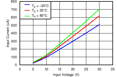 Figure 2. Input Supply Current vs Supply Voltage
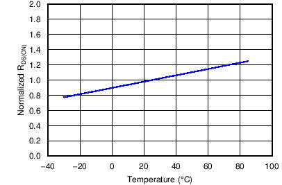
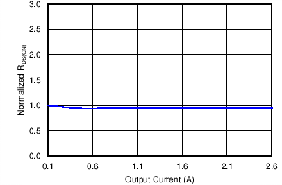 Figure 4. Normalized RDS(ON) vs Output Current
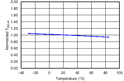 Figure 6. Normalized TDELAY
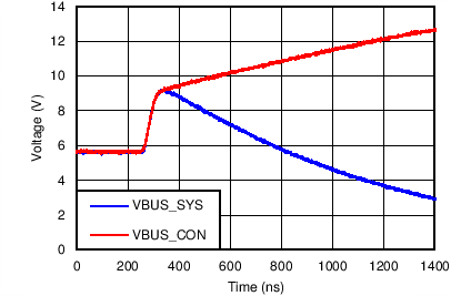
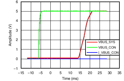 Figure 8. Power Up With 2.2 µF on VBUS_SYS
