|
What are Current
Sense Amplifiers?
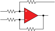
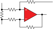
Current sense
amplifiers, also called current shunt monitors, are specialized
differential amplifiers with a precisely matched resistive gain
network with the following characteristics:
- Designed to
monitor the current flow by measuring the voltage drop
across a sense element, typically a shunt resistor.
- Tend to be
easier to use, more precise, and less prone to noise.
- Support
currents from 10s of μA to 100s of A.
- Natively-support common-mode voltages from –16 to +80 V and
with additional circuitry up to 100s of volts.
System Benefits
Addressed by Using Current Sense Amplifiers
- Real-time
overcurrent protection
- Current and power
monitoring for system optimization
- Current
measurement for closed-loop feedback
Key
Parameters
| Common Mode
Range |
This specification defines the
DC voltage range at the input of an amplifier with
respect to ground. Current sense amplifiers are
typically designed to support common-mode voltages
well beyond the chip supply voltage. For example,
the INA240 is capable of supporting a common-mode
voltage between –4 V to +80 V while running on a
supply as low as 2.7 V. |
| Offset
Voltage |
This is a differential DC error
at the input of the amplifier. Historically, to
reduce the impact of amplifiers with high offsets,
larger value shunt resistors were used to increase
the measured voltage drop. Today, TI is able to
offer current sense amplifiers with offsets as low
as 10 μV, enabling higher-precision measurements
at low currents and allowing the use of smaller
value shunt resistors for improved system
efficiency. |
| Gain |
Current sense amplifiers come
with various gain options that have robust
performance over temperature and process
variations by integrating a precisely-matched
resistive gain network. The gain options for fixed
gain amplifiers vary from 0.125 V/V to 1000 V/V
with gain errors as low as 0.01%. |
| Temperature
Stability |
Current sense amplifiers
integrate the amplifier along with all the
gain-setting resistors which enables small and
unified temperature drift. This allows for robust
current measurements across the whole specified
temperature range. The achieved temperature
stability is one of the key advantages current
sense amplifiers have over discrete
implementations. |
|