SBOA334A January 2019 – December 2020 OPA182 , OPA186 , OPA187 , OPA188 , OPA189 , OPA2182 , OPA2186 , OPA2187 , OPA2189 , OPA2387 , OPA333 , OPA387 , OPA388 , OPA4182 , OPA4186 , OPA4187 , OPA4387 , TLV2186
Application Brief
Precision Amplifiers
The accuracy of weigh scales is affected by several factors, including input offset voltage drift, vibration RFI, and electromagnetic interference (EMI). The EMI sources can emanate from light, long wires, relays, cell phones, and other electronic equipment in the vicinity. Weigh-scale accuracy is affected by radiated and conducted undesirable signals because these signals can cause erroneous readings, thereby impacting the sensitivity of the apparatus.
Benefits of EMI Hardened Zero-Drift Amplifiers in Weigh Scales
Zero-drift amplifiers provide the advantage of very low input offset voltage, as well as very low offset drift. Errors attributed to the input offset voltage and offset drift affect the accuracy of the weigh scale.
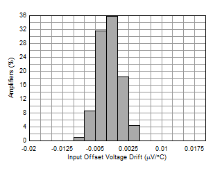
For example, a 16-bit analog-to-digital converter (ADC) with a full-scale voltage range of 10 V yields 1 LSB of 153 µV. An amplifier with an offset voltage of 0.5 mV is well above 1 LSB. To avoid quantization errors and maintain linearity, select a precision amplifier that yields ½ LSB. A zero-drift amplifier such as the OPA2182 has 0.45 µV of offset voltage and 0.003 µV of offset voltage drift, as shown in Figure 1-1.
 Figure 1-1 OPA2182 Input Offset Drift
 At 70°C, the total offset error (with drift) amounts to 0.58 µV; well below 76 µV.
Another benefit of zero-drift amplifiers is very-low flicker noise (1/f), even when compared to bipolar input op amps. The 1/f component can be a dominant source of error, and is particularly important in low-frequency bands because the impact of the op amp noise can be detrimental to the design. Noise causes a loss of digital counts and degrades ENOB performance, thereby reducing weigh scale accuracy. The ulta low offset OPA2387 has a 1/f noise (peak to peak) of 177 nV/√Hz.
Advantages of EMI-Hardened Op Amps
To avoid problems associated with EMI, precautionary measures must be taken. These measures include shielding, proper grounding, and filtering. Passive filters at the input and output of the amplifier are not a trivial task. A simple low-pass RC filter, whether at the input or output, is likely to affect the dynamic performance of the amplifier. The most effective way to reject RF and EMI signals is to select op amps with integrated filters.
Texas Instruments precision amplifiers are designed with integrated filters that are closely matched on silicon. The additional filters reduce errors through the signal path feeding into the ADC. EMIRR plots are provided in the product data sheet and, much like PSRR or CMRR, these graphs show the rejection over a frequency band.
To better understand how EMI-hardened amplifiers reduce errors, consider this example:
Suppose a non-EMI-hardened op amp inherently provides 50 dB of rejection, is set up in a gain of 100, and interfaces with a 16‑bit ADC with a full-scale voltage range of 5 V.
Next, assume an RF signal of –20 dBV (0.1 V) at the input of the amplifier. A quick computation yields 0.31 mV at the input or 0.1 V / 10(50 / 20). Multiplying by a gain of 101 gives 32 mV. With a 5‑V full-scale voltage range and a 16-bit ADC we have 5 / (216) = 76 µV as 1 LSB.
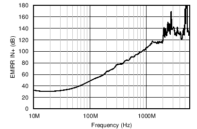
Taking the initial 32 mV and dividing by 76 µV yields approximately 420, which represents the loss of digital counts. Selecting an amplifier like the zero-drift OPA187 provides 100 dB of EMIRR at 1 GHz, as shown in Figure 1-2.
The following steps determine how much improvement can be achieved by using the OPA187.
First, compute the shift at the output as:
0.1 V / (105) × 101, which gives 0.1 mV at
the output of the amplifier. To find the loss of counts, simply take 0.1 mV and
divide by 76 µV, which represents 1 LSB for 16 bits with a full-scale voltage range
of 5 V. Write the equation as (0.1E-3 / (5 / 65536)), which yields 1.3 counts. An
extraordinary improvement without compromise!
Check out this clip in TI's video library for some additional interesting information: How to avoid electromagnetic interference (EMI).
 Figure 1-2 OPA187 EMIRR IN+ vs
Frequency
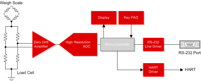
 Figure 1-3 Typical Block Diagram of a
Precision Weigh Scale
Figure 1-3 Typical Block Diagram of a
Precision Weigh Scale| Device | Unity Gain Bandwidth | Description |
|---|---|---|
| OPA189 | 14 MHz | 14-MHz, MUX-Friendly, Low-Noise, Zero-Drift, RRO, CMOS, Precision Operational Amplifier |
| OPA188 | 2 MHz | Precision, Low-Noise, Rail-to-Rail Output, 36-V, Zero-Drift Operational Amplifier |
5 MHz | Industry’s Lowest Offset Drift Operational Amplifier | |
0.55MHz | Low Power, High Voltage Zero Drift Operational Amplifier | |
0.75 MHz | 24V, Cost Optimized Low Power Zero Drift Operational Amplifier | |
| OPA388 | 10 MHz | 10-MHz, CMOS, Zero-Drift, Zero-Crossover, True RRIO, Precision Operational Amplifier |
5.7 MHz | Ultra High Precision, Low Input Bias Current Zero Drift Operational Amplifier | |
350 kHz | Zero-Drift microPower Operational Amplifier |