-
ADS124x 24-Bit, 2-kSPS, Analog-To-Digital Converters With Programmable Gain Amplifier (PGA) For Sensor Measurement
- 1 Features
- 2 Applications
- 3 Description
- 4 Revision History
- 5 Device Comparison Table
- 6 Pin Configuration and Functions
- 7 Specifications
- 8 Parameter Measurement Information
-
9 Detailed Description
- 9.1 Overview
- 9.2 Functional Block Diagram
- 9.3
Feature Description
- 9.3.1 ADC Input and Multiplexer
- 9.3.2 Low-Noise PGA
- 9.3.3 Clock Source
- 9.3.4 Modulator
- 9.3.5 Digital Filter
- 9.3.6 Voltage Reference Input
- 9.3.7 Internal Voltage Reference
- 9.3.8 Excitation Current Sources
- 9.3.9 Sensor Detection
- 9.3.10 Bias Voltage Generation
- 9.3.11 General-Purpose Digital I/O
- 9.3.12 System Monitor
- 9.4 Device Functional Modes
- 9.5
Programming
- 9.5.1 Serial Interface
- 9.5.2 Data Format
- 9.5.3
Commands
- 9.5.3.1 WAKEUP (0000 000x)
- 9.5.3.2 SLEEP (0000 001x)
- 9.5.3.3 SYNC (0000 010x)
- 9.5.3.4 RESET (0000 011X)
- 9.5.3.5 RDATA (0001 001x)
- 9.5.3.6 RDATAC (0001 010x)
- 9.5.3.7 SDATAC (0001 011x)
- 9.5.3.8 RREG (0010 rrrr, 0000 nnnn)
- 9.5.3.9 WREG (0100 rrrr, 0000 nnnn)
- 9.5.3.10 SYSOCAL (0110 0000)
- 9.5.3.11 SYSGCAL (0110 0001)
- 9.5.3.12 SELFOCAL (0110 0010)
- 9.5.3.13 NOP (1111 1111)
- 9.5.3.14 Restricted Command (1111 0001)
- 9.6
Register Maps
- 9.6.1 ADS1246 Register Map
- 9.6.2
ADS1246 Detailed Register Definitions
- 9.6.2.1 BCS—Burn-out Current Source Register (offset = 00h) [reset = 01h]
- 9.6.2.2 VBIAS—Bias Voltage Register (offset = 01h) [reset = 00h]
- 9.6.2.3 MUX—Multiplexer Control Register (offset = 02h) [reset = x0h]
- 9.6.2.4 SYS0—System Control Register 0 (offset = 03h) [reset = 00h]
- 9.6.2.5 OFC—Offset Calibration Coefficient Registers (offset = 04h, 05h, 06h) [reset = 00h, 00h, 00h]
- 9.6.2.6 FSC—Full-Scale Calibration Coefficient Registers (offset = 07h, 08h, 09h) [reset = PGA dependent]
- 9.6.2.7 ID—ID Register (offset = 0Ah) [reset = x0h]
- 9.6.3 ADS1247 and ADS1248 Register Map
- 9.6.4
ADS1247 and ADS1248 Detailed Register Definitions
- 9.6.4.1 MUX0—Multiplexer Control Register 0 (offset = 00h) [reset = 01h]
- 9.6.4.2 VBIAS—Bias Voltage Register (offset = 01h) [reset = 00h]
- 9.6.4.3 MUX1—Multiplexer Control Register 1 (offset = 02h) [reset = x0h]
- 9.6.4.4 SYS0—System Control Register 0 (offset = 03h) [reset = 00h]
- 9.6.4.5 OFC—Offset Calibration Coefficient Register (offset = 04h, 05h, 06h) [reset = 00h, 00h, 00h]
- 9.6.4.6 FSC—Full-Scale Calibration Coefficient Register (offset = 07h, 08h, 09h) [reset = PGA dependent]
- 9.6.4.7 IDAC0—IDAC Control Register 0 (offset = 0Ah) [reset = x0h]
- 9.6.4.8 IDAC1—IDAC Control Register 1 (offset = 0Bh) [reset = FFh]
- 9.6.4.9 GPIOCFG—GPIO Configuration Register (offset = 0Ch) [reset = 00h]
- 9.6.4.10 GPIODIR—GPIO Direction Register (offset = 0Dh) [reset = 00h]
- 9.6.4.11 GPIODAT—GPIO Data Register (offset = 0Eh) [reset = 00h]
-
10Application and Implementation
- 10.1
Application Information
- 10.1.1 Serial Interface Connections
- 10.1.2 Analog Input Filtering
- 10.1.3 External Reference and Ratiometric Measurements
- 10.1.4 Establishing a Proper Common-Mode Input Voltage
- 10.1.5 Isolated (or Floating) Sensor Inputs
- 10.1.6 Unused Inputs and Outputs
- 10.1.7 Pseudo Code Example
- 10.1.8 Channel Multiplexing Example
- 10.1.9 Power-Down Mode Example
- 10.2 Typical Applications
- 10.3 Do's and Don'ts
- 10.1
Application Information
- 11Power-Supply Recommendations
- 12Layout
- 13Device and Documentation Support
- 14Mechanical, Packaging, and Orderable Information
- IMPORTANT NOTICE
ADS124x 24-Bit, 2-kSPS, Analog-To-Digital Converters With Programmable Gain Amplifier (PGA) For Sensor Measurement
1 Features
- Programmable Data Rates Up to 2 kSPS
- Single-Cycle Settling for All Data Rates
- Simultaneous 50-Hz and 60-Hz Rejection at 20 SPS
- Analog Multiplexer With 8 (ADS1248) and 4 (ADS1247) Independently Selectable Inputs
- Low-Noise PGA: 48 nVRMS at PGA = 128
- Dual-Matched Programmable Excitation Current Sources
- Low-Drift Internal 2.048-V Reference:
10 ppm/°C (Maximum) - Sensor Burn-Out Detection
- 4 or 8 General-Purpose I/Os (ADS1247, ADS1248)
- Internal Temperature Sensor
- Power Supply and VREF Monitoring (ADS1247, ADS1248)
- Self and System Calibration
- SPI™-Compatible Serial Interface
- Analog Supply: Unipolar (2.7 V to 5.25 V) and Bipolar (±2.5 V) Operation
- Digital Supply: 2.7 V to 5.25 V
2 Applications
- Temperature Sensor Measurements:
- RTDs, Thermocouples, and Thermistors
- Pressure Measurements
- Flow Meters
- Factory Automation and Process Controls
3 Description
The ADS1246, ADS1247, and ADS1248 devices are precision, 24-bit analog-to-digital converters (ADCs) that include many integrated features to reduce system cost and component count for sensor measurement applications. The devices feature a low-noise, programmable gain amplifier (PGA), a precision delta-sigma (ΔΣ) ADC with a single-cycle settling digital filter, and an internal oscillator. The ADS1247 and ADS1248 devices also provide a built-in, low-drift voltage reference, and two matched programmable excitation current sources (IDACs).
An input multiplexer supports four differential inputs for the ADS1248, two for the ADS1247, and one for the ADS1246. In addition, the multiplexer integrates sensor burn-out detection, voltage bias for thermocouples, system monitoring, and general purpose digital I/Os (ADS1247 and ADS1248). The PGA provides selectable gains up to 128 V/V. These features provide a complete front-end solution for temperature sensor measurement applications including thermocouples, thermistors, and resistance temperature detectors (RTDs) and other small signal measurements including resistive bridge sensors. The digital filter settles in a single cycle to support fast channel cycling when using the input multiplexer and provides data rates up to 2 kSPS. For data rates of 20 SPS or less, both 50-Hz and 60-Hz interference are rejected by the filter.
Device Information(1)
| PART NUMBER | PACKAGE | BODY SIZE (NOM) |
|---|---|---|
| ADS1246 | TSSOP (16) | 5.00 mm × 4.40 mm |
| ADS1247 | TSSOP (20) | 6.50 mm × 4.40 mm |
| ADS1248 | TSSOP (28) | 9.70 mm × 4.40 mm |
- For all available packages, see the orderable addendum at the end of the datasheet.
4 Revision History
Changes from G Revision (October 2011) to H Revision
- Added ESD Ratings table, Feature Description section, Device Functional Modes, Application and Implementation section, Power Supply Recommendations section, Layout section, Device and Documentation Support section, and Mechanical, Packaging, and Orderable Information sectionGo
- Updated Features and Description sections to include use in applications other than temperature measurementGo
- Edited Device Comparison Table to include ADS1146, ADS1147, and ADS1148; changed title, deleted footnoteGo
- Merged all Pin Functions into one table, changed IOUT1 and IOUT2 to IEXC1 and IEXC2 to match figuresGo
- Changed compliance voltage for excitation current sources in Electrical Characteristics, now refers to Figure 41 and Figure 42; changed initial error and initial mismatch to absolute error and absolute mismatchGo
- Re-ordered elements in Timing Requirements tables, changed timing references to tCLKGo
- Changed order of Typical Characteristics curves to match order in Electrical Characteristics tableGo
- Added cross-reference for Equation 1 in Noise Performance sectionGo
- Corrected values in Table 2Go
- Modified Low-Noise PGA section to add more detail; added Table 7; added PGA Common-Mode Voltage Requirements and PGA Common-Mode Voltage Calculation Example sectionsGo
- Added fCLK/fMOD column to Table 9Go
- Added cross-reference for Equation 15 to Power-Supply Monitor sectionGo
- Added cross-reference for Equation 16 to External Voltage Reference Monitor sectionGo
- Added Device Functional Modes sectionGo
- Corrected values in Table 15 to remove extra 0 in 800000hGo
- Added text to Chip Select section to say that SCLK will force DRDY high, even with CS highGo
- Added text to Data Output and Data Ready section to say that stop read data continuous mode is not compatible with DRDY MODE set to 1Go
- Modified Figure 74 and Figure 75 to better show DIN transitions with respect to SCLK; replaced Figure 76 to better show full command and DRDY/DOUT falling with NOP.Go
- Added more infomation to Data Format section; added Figure 77Go
- Added cross-reference for Figure 78 to Commands sectionGo
- Modified Figure 78 to include CS status through SLEEP and WAKEUP commandGo
- Updated Figure 79 and Figure 80 to show start of command executionGo
- Added cross-reference for Figure 83 to Commands sectionGo
- Removed figure for SDATAC (Stop Read Data Continuous) commandGo
- Updated Figure 85 to show MUX1 as the start of the data byte for the given command and register locationGo
- Updated Figure 86 to show start of calibration timingGo
- Updated Register Maps section to new formatGo
- Updated Application Information section. Included new typical applications for Ratiometric 3-Wire RTD Measurement System and K-Type Thermocouple Measurement (–200°C to +1250°C) with Cold-Junction CompensationGo
- Updated Figure 112 and Figure 113 to better show timing informationGo
- Removed Hardware-Compensated 3-Wire RTD Measurement application sectionGo
Changes from F Revision (June 2011) to G Revision
Changes from E Revision (December, 2010) to F Revision
- Added footnote to Full-scale input voltage specification in Electrical Characteristics tableGo
- Added test condition for INL parameter of Electrical CharacteristicsGo
- Added tCSPW to minimum specification in Timing Characteristics for Figure 1Go
- Updated Figure 1 to show tCSPW timingGo
- Corrected grid and axis values for Figure 29Go
- Corrected grid and axis values for Figure 30Go
- Updated Figure 51Go
- Added details to Bias Voltage Generation sectionGo
- Corrected Table 14Go
- Added details to Calibration sectionGo
- Added Equation 18 to Calibration sectionGo
- Added section to Calibration CommandsGo
- Added details to Digital Interface sectionGo
- Added Restricted command space to Table 19Go
5 Device Comparison Table
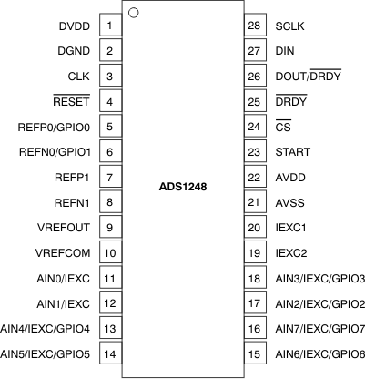
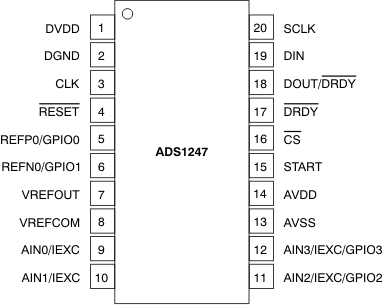
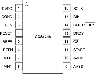
6 Pin Configuration and Functions


Pin Functions
| PIN | TYPE(1) | DESCRIPTION(2) | |||
|---|---|---|---|---|---|
| NAME | ADS1248 (TSSOP-28) |
ADS1247 (TSSOP-20) |
ADS1246 (TSSOP-16) |
||
| AIN0/IEXC | 11 | 9 | — | I | Analog input 0, optional excitation current output |
| AIN1/IEXC | 12 | 10 | — | I | Analog input 1, optional excitation current output |
| AIN2/IEXC/GPIO2 | 17 | 11 | — | I/O | Analog input 2, optional excitation current output, or general-purpose digital input/output pin 2 |
| AIN3/IEXC/GPIO3 | 18 | 12 | — | I/O | Analog input 3, optional excitation current output, or general-purpose digital input/output pin 3 |
| AIN4/IEXC/GPIO4 | 13 | — | — | I/O | Analog input 4, optional excitation current output, or general-purpose digital input/output pin 4 |
| AIN5/IEXC/GPIO5 | 14 | — | — | I/O | Analog input 5, optional excitation current output, or general-purpose digital input/output pin 5 |
| AIN6/IEXC/GPIO6 | 15 | — | — | I/O | Analog input 6, optional excitation current output, or general-purpose digital input/output pin 6 |
| AIN7/IEXC/GPIO7 | 16 | — | — | I/O | Analog input 7, optional excitation current output, or general-purpose digital input/output pin 7 |
| AINN | — | — | 8 | I | Negative analog input |
| AINP | — | — | 7 | I | Positive analog input |
| AVDD | 22 | 14 | 10 | P | Positive analog power supply, connect a 0.1-μF capacitor to AVSS |
| AVSS | 21 | 13 | 9 | P | Negative analog power supply |
| CLK | 3 | 3 | 3 | I | External clock input, tie to DGND to activate the internal oscillator |
| CS | 24 | 16 | 12 | I | Chip select (active low) |
| DGND | 2 | 2 | 2 | G | Digital ground |
| DIN | 27 | 19 | 15 | I | Serial data input |
| DOUT/DRDY | 26 | 18 | 14 | O | Serial data output or data output combined with data ready |
| DRDY | 25 | 17 | 13 | O | Data ready (active low) |
| DVDD | 1 | 1 | 1 | P | Digital power supply, connect a 0.1-μF capacitor to DGND |
| IEXC1 | 20 | — | — | O | Excitation current output 1 |
| IEXC2 | 19 | — | — | O | Excitation current output 2 |
| REFN | — | — | 6 | I | Negative external reference input |
| REFN0/GPIO1 | 6 | 6 | — | I/O | Negative external reference input 0, or general-purpose digital input/output pin 1 |
| REFN1 | 8 | — | — | I | Negative external reference input 1 |
| REFP | — | — | 5 | I | Positive external reference input |
| REFP0/GPIO0 | 5 | 5 | — | I/O | Positive external reference input 0, or general-purpose digital input/output pin 0 |
| REFP1 | 7 | — | — | I | Positive external reference input 1 |
| RESET | 4 | 4 | 4 | I | Reset (active low) |
| SCLK | 28 | 20 | 16 | I | Serial clock input |
| START | 23 | 15 | 11 | I | Conversion start |
| VREFCOM | 10 | 8 | — | O | Negative internal reference voltage output, connect to AVSS when using a unipolar supply or to the mid-voltage of the power supply when using a bipolar supply |
| VREFOUT | 9 | 7 | — | O | Positive internal reference voltage output, connect a capacitor in the range of 1-μF to 47-μF to VREFCOM |
