-
ADS8320 16-Bit, High-Speed, 2.7-V to 5-V microPower Sampling Analog-to-Digital Converter
- 1 Features
- 2 Applications
- 3 Description
- 4 Revision History
- 5 Pin Configuration and Functions
- 6 Specifications
- 7 Detailed Description
- 8 Application and Implementation
- 9 Power Supply Recommendations
- 10Layout
- 11Device and Documentation Support
- 12Mechanical, Packaging, and Orderable Information
- IMPORTANT NOTICE
ADS8320 16-Bit, High-Speed, 2.7-V to 5-V microPower Sampling Analog-to-Digital Converter
1 Features
- 100-kHz Sampling Rate
-
microPower:
- 1.8 mW at 100 kHz and 2.7 V
- 0.3 mW at 10 kHz and 2.7 V
- Power Down: 3 µA (Maximum)
- 8-Pin VSSOP Package
- Pin-Compatible to ADS7816 and ADS7822
- Serial (SPI™/SSI) Interface
2 Applications
- Battery-Operated Systems
- Remote Data Acquisition
- Isolated Data Acquisition
- Simultaneous Sampling, Multichannel Systems
- Industrial Controls
- Robotics
- Vibration Analysis
3 Description
The ADS8320 device is a 16-bit, sampling analog-to-digital (A/D) converter with ensured specifications over a 2.7-V to 5.25-V supply range. It requires very little power even when operating at the full 100-kHz data rate. At lower data rates, the high speed of the device enables it to spend most of its time in the power-down mode. The average power dissipation is less than 100 mW at 10-kHz data rate.
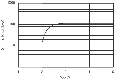
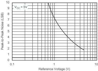
The ADS8320 also features operation from 2 V to 5.25 V, a synchronous serial (SPI/SSI compatible) interface, and a differential input. The reference voltage can be set to any level within the range of 500 mV to VCC.
Ultra-low power and small size make the ADS8320 ideal for portable and battery-operated systems. It is also a perfect fit for remote data acquisition modules, simultaneous multi-channel systems, and isolated data acquisition. The ADS8320 is available in an
8-pin VSSOP package.
Device Information(1)
| PART NUMBER | PACKAGE | BODY SIZE (NOM) |
|---|---|---|
| ADS8320 | VSSOP (8) | 3.00 mm × 3.00 mm |
- For all available packages, see the orderable addendum at the end of the data sheet.
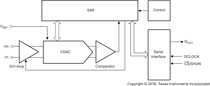
Block Diagram
4 Revision History
Changes from D Revision (March 2007) to E Revision
- Added ESD Ratings table, Feature Description section, Device Functional Modes, Application and Implementation section, Power Supply Recommendations section, Layout section, Device and Documentation Support section, and Mechanical, Packaging, and Orderable Information section Go
- Added Thermal Information tableGo
- Changed Application Circuits section To: Typical Connection DiagramGo
5 Pin Configuration and Functions
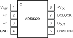
Pin Functions
| PIN | TYPE(1) | DESCRIPTION | |
|---|---|---|---|
| NO. | NAME | ||
| 1 | VREF | AI | Reference input |
| 2 | +In | AI | Noninverting input |
| 3 | –In | AI | Inverting input: Connect to ground or to remote ground sense point. |
| 4 | GND | GND | Ground |
| 5 | CS/SHDN | DI | Chip select when LOW; Shutdown mode when HIGH. |
| 6 | DOUT | DO | The serial output data word is comprised of 16 bits of data. In operation the data is valid on the falling edge of DCLOCK. The second clock pulse after the falling edge of CS enables the serial output. After one null bit the data is valid for the next 16 edges. |
| 7 | DCLOCK | DI | Data clock synchronizes the serial data transfer and determines conversion speed. |
| 8 | +VCC | PWR | Power supply |
6 Specifications
6.1 Absolute Maximum Ratings
over operating free-air temperature range (unless otherwise noted)(1)| MIN | MAX | UNIT | ||
|---|---|---|---|---|
| VCC | 6 | V | ||
| Analog input | –0.3 | VCC + 0.3 | V | |
| Logic input | –0.3 | 6 | °C | |
| External reference voltage | 5.5 | V | ||
| Input current to any pin except supply | ±10 | mA | ||
| Case temperature | 100 | °C | ||
| Junction temperature | 150 | °C | ||
| Storage temperature, Tstg | 125 | °C | ||
6.2 ESD Ratings
| VALUE | UNIT | |||
|---|---|---|---|---|
| V(ESD) | Electrostatic discharge | Human-body model (HBM), per ANSI/ESDA/JEDEC JS-001(1) | ±2000 | V |
| Charged-device model (CDM), per JEDEC specification JESD22-C101(2) | ±1000 | |||
6.3 Recommended Operating Conditions
over operating free-air temperature range (unless otherwise noted)| MIN | NOM | MAX | UNIT | ||
|---|---|---|---|---|---|
| Supply voltage, VCC to GND | Low voltage levels | 2.7 | 3.3 | V | |
| 5-V logic levels | 4.75 | 5 | 5.25 | ||
| Reference input voltage, VREF | 0.5 | VCC | V | ||
| Analog input voltage | –IN to GND | –0.1 | 0 | 0.5 | V |
| +IN to GND | –0.1 | VCC + 0.1 | |||
| +IN to – (–IN) | 0 | VREF | |||
| Operating temperature, TA | –40 | 85 | °C | ||
6.4 Thermal Information
| THERMAL METRIC(1) | ADS8320 | UNIT | |
|---|---|---|---|
| DGK (VSSOP) | |||
| 8 PINS | |||
| RθJA | Junction-to-ambient thermal resistance | 163.1 | °C/W |
| RθJC(top) | Junction-to-case (top) thermal resistance | 56.6 | °C/W |
| RθJB | Junction-to-board thermal resistance | 83.4 | °C/W |
| ψJT | Junction-to-top characterization parameter | 6.7 | °C/W |
| ψJB | Junction-to-board characterization parameter | 82 | °C/W |
| RθJC(bot) | Junction-to-case (bottom) thermal resistance | — | °C/W |
6.5 Electrical Characteristics: VCC = 5 V
at –40°C to 85°C, VREF = 5 V, –IN = GND, fSAMPLE = 100 kHz, and fCLK = 24 × fSAMPLE (unless otherwise noted)| PARAMETER | TEST CONDITIONS | MIN | TYP | MAX | UNIT | ||||
|---|---|---|---|---|---|---|---|---|---|
| RESOLUTION | |||||||||
| Resolution | 16 | Bits | |||||||
| ANALOG INPUT | |||||||||
| Full-scale input span | +In – (–In) | 0 | VREF | V | |||||
| Absolute input | +In | –0.1 | VCC + 0.1 | V | |||||
| –In | –0.1 | 1 | |||||||
| Capacitance | 45 | pF | |||||||
| Leakage current | 1 | nA | |||||||
| SYSTEM PERFORMANCE | |||||||||
| No missing codes | ADS8320E | 14 | Bits | ||||||
| ADS8320EB | 15 | ||||||||
| Integral linearity error | ADS8320E | ±0.008% | ±0.018% | FSR | |||||
| ADS8320EB | ±0.006% | ±0.012% | |||||||
| Offset error | ADS8320E | ±1 | ±2 | mV | |||||
| ADS8320EB | ±0.5 | ±1 | |||||||
| Offset temperature drift | ±3 | µV/°C | |||||||
| Gain error | ADS8320E | ±0.05% | FSR | ||||||
| ADS8320EB | ±0.024% | ||||||||
| Gain error temperature drift | ±0.3 | ppm/°C | |||||||
| Noise | 20 | µVrms | |||||||
| Power-supply rejection ratio | 4.7 V < VCC < 5.25 V | 3 | LSB(1) | ||||||
| SAMPLING DYNAMICS | |||||||||
| Conversion time | 16 | Clock Cycles | |||||||
| Acquisition time | 4.5 | Clock Cycles | |||||||
| Throughput rate | 100 | kHz | |||||||
| Clock frequency | 0.024 | 2.4 | MHz | ||||||
| DYNAMIC CHARACTERISTICS | |||||||||
| Total harmonic distortion | VIN = 5 VP-P at 10 kHz | ADS8320E | –84 | dB | |||||
| ADS8320EB | –86 | ||||||||
| SINAD | VIN = 5 VP-P at 10 kHz | ADS8320E | 82 | dB | |||||
| ADS8320EB | 84 | ||||||||
| Spurious-free dynamic | VIN = 5 VP-P at 10 kHz | ADS8320E | 84 | dB | |||||
| ADS8320EB | 86 | ||||||||
| SNR | ADS8320E | 90 | dB | ||||||
| ADS8320EB | 92 | ||||||||
| REFERENCE INPUT | |||||||||
| Voltage | 0.5 | VCC | V | ||||||
| Resistance | CS = GND, fSAMPLE = 0 Hz | 5 | GΩ | ||||||
| CS = VCC | 5 | ||||||||
| Current drain | 40 | 80 | µA | ||||||
| fSAMPLE = 0 Hz | 0.8 | ||||||||
| CS = VCC | 0.1 | 3 | |||||||
| DIGITAL INPUT/OUTPUT | |||||||||
| Logic family | CMOS | ||||||||
| Logic levels | VIH | IIH = 5 µA | 3 | VCC + 0.3 | V | ||||
| VIL | IIL = 5 µA | –0.3 | 0.8 | ||||||
| VOH | IOH = –250 µA | 4 | |||||||
| VOL | IOL = 250 µA | 0.4 | |||||||
| Data format | Straight Binary | ||||||||
| POWER SUPPLY REQUIREMENTS | |||||||||
| VCC | Specified performance | 4.75 | 5.25 | V | |||||
| VCC(2) | 2 | 5.25 | V | ||||||
| Quiescent current | 900 | 1700 | µA | ||||||
| fSAMPLE = 10 kHz(3)(4) | 200 | ||||||||
| Power dissipation | 4.5 | 8.5 | mW | ||||||
| Power down | CS = VCC | 0.3 | 3 | µA | |||||
6.6 Electrical Characteristics: VCC = 2.7 V
at –40°C to 85°C, VREF = 5 V, –IN = GND, fSAMPLE = 100 kHz, and fCLK = 24 × fSAMPLE (unless otherwise noted)| PARAMETER | TEST CONDITIONS | MIN | TYP | MAX | UNIT | |||
|---|---|---|---|---|---|---|---|---|
| RESOLUTION | ||||||||
| Resolution | 16 | Bits | ||||||
| ANALOG INPUT | ||||||||
| Full-scale input span | +In – (–In) | 0 | VREF | V | ||||
| Absolute input | +In | –0.1 | VCC + 0.1 | V | ||||
| –In | –0.1 | 0.5 | ||||||
| Capacitance | 45 | pF | ||||||
| Leakage current | 1 | nA | ||||||
| SYSTEM PERFORMANCE | ||||||||
| No missing codes | ADS8320E | 14 | Bits | |||||
| ADS8320EB | 15 | |||||||
| Integral linearity error | ADS8320E | ±0.008% | ±0.018% | FSR | ||||
| ADS8320EB | ±0.006% | ±0.012% | ||||||
| Offset error | ADS8320E | ±1 | ±2 | mV | ||||
| ADS8320EB | ±0.5 | ±1 | ||||||
| Offset temperature drift | ±3 | µV/°C | ||||||
| Gain error | ADS8320E | ±0.05% | FSR | |||||
| ADS8320EB | ±0.024% | |||||||
| Gain error temperature drift | ±0.3 | ppm/°C | ||||||
| Noise | 20 | ppm/°C | ||||||
| Power-supply rejection ratio | 2.7 V < VCC < 3.3 V | 3 | LSB(1) | |||||
| SAMPLING DYNAMICS | ||||||||
| Conversion time | 16 | Clock Cycles | ||||||
| Acquisition time | 4.5 | Clock Cycles | ||||||
| Throughput rate | 100 | kHz | ||||||
| Clock frequency | 0.024 | 2.4 | MHz | |||||
| DYNAMIC CHARACTERISTICS | ||||||||
| Total harmonic distortion | VIN = 2.7 VP-P at 1 kHz | ADS8320E | –86 | dB | ||||
| ADS8320EB | –88 | |||||||
| SINAD | VIN = 2.7 VP-P at 1 kHz | ADS8320E | 84 | dB | ||||
| ADS8320EB | 86 | |||||||
| Spurious-free dynamic | VIN = 2.7 VP-P at 1 kHz | ADS8320E | 86 | dB | ||||
| ADS8320EB | 88 | |||||||
| SNR | ADS8320E | 88 | dB | |||||
| ADS8320EB | 90 | |||||||
| REFERENCE INPUT | ||||||||
| Voltage | 0.5 | VCC | V | |||||
| Resistance | CS = GND, fSAMPLE = 0 Hz | 5 | GΩ | |||||
| CS = VCC | 5 | |||||||
| Current drain | 20 | 50 | µA | |||||
| CS = VCC | 0.1 | 3 | ||||||
| DIGITAL INPUT/OUTPUT | ||||||||
| Logic Family | CMOS | |||||||
| Logic levels | VIH | IIH = 5 µA | 2 | VCC + 0.3 | V | |||
| VIL | IIL = 5 µA | –0.3 | 0.8 | |||||
| VOH | IOH = –250 µA | 2.1 | ||||||
| VOL | IOL = 250 µA | 0.4 | ||||||
| Data format | Straight Binary | |||||||
| POWER SUPPLY REQUIREMENTS | ||||||||
| VCC | Specified performance | 2.7 | 3.3 | V | ||||
| VCC(3) | 2 | 5.25 | V | |||||
| See(2) | 2 | 2.7 | ||||||
| Quiescent current | 650 | 1300 | µA | |||||
| fSAMPLE = 10 kHz(4)(5) | 100 | |||||||
| Power dissipation | 1.8 | 3.8 | mW | |||||
| Power down | CS = VCC | 0.3 | 3 | µA | ||||
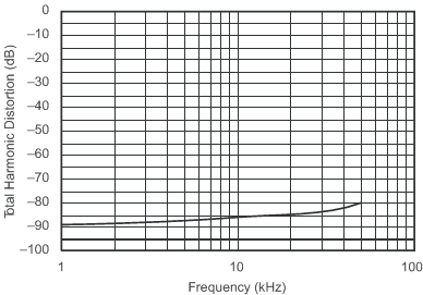
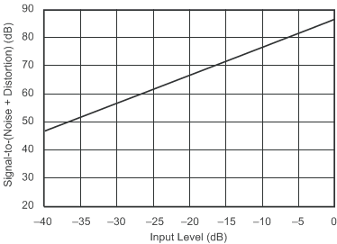
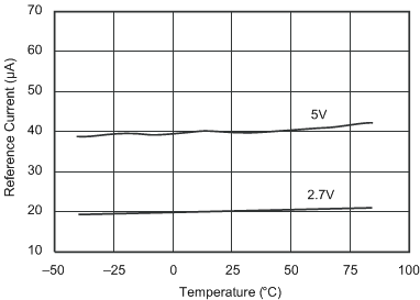
6.7 Typical Characteristics
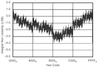


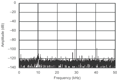
FIN = 10.120 kHz, –0.3 dB)

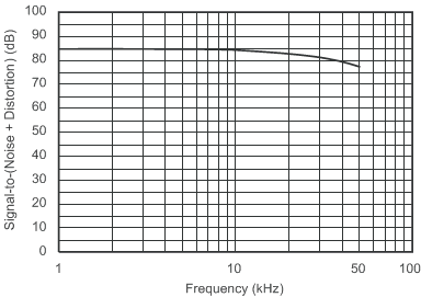

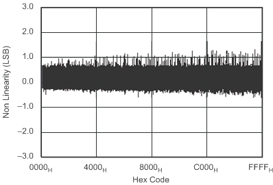
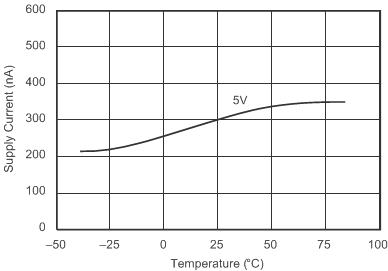
Code (25°C)
